
Close Menu
  • News
    • Medical
    • Nanomaterials
    • AI & Robotics
    • 2D Materials
    • Metamaterials
    • Nanoelectronics
    • ETF’s
    • Medicine
  • Environment
    • Earth.com
    • TreeHugger
    • Nanomuscle
  • Beauty
    • Makeupanalysis
What's Hot

Biomass-Derived Nanomaterials Offer a Greener Route to Pollution Cleanup

September 1, 2026

Nanozyme Aptasensors Show Promise for Faster Food, Health, and Environmental Testing

September 1, 2026

Researchers Solve Two Major Problems Holding Back SiC Electronics

September 1, 2026
Facebook X (Twitter) Instagram
  • Contact Us
  • Privacy Policy
  • Terms & Conditions
Facebook X (Twitter) Instagram
Elnano – Global Innovative Nanotechnology SolutionsElnano – Global Innovative Nanotechnology Solutions
  • News
    • Medical
    • Nanomaterials
    • AI & Robotics
    • 2D Materials
    • Metamaterials
    • Nanoelectronics
    • ETF’s
    • Medicine
  • Environment
    • Earth.com
    • TreeHugger
    • Nanomuscle
  • Beauty
    • Makeupanalysis
Elnano – Global Innovative Nanotechnology SolutionsElnano – Global Innovative Nanotechnology Solutions
Home » Scientists Marry DNA Origami and 2D Materials to Make Nanoelectronics
Nanoelectronics

Scientists Marry DNA Origami and 2D Materials to Make Nanoelectronics

April 3, 2026No Comments3 Mins Read
Share
Facebook Twitter LinkedIn Pinterest Email

Skoltech researchers and their colleagues from Ludwig Maximilian University of Munich, Germany, Nanjing University of China, and the National Institute for Materials Science of Japan have developed a method for depositing organic molecules on a two-dimensional semiconductor in a highly controlled manner. Tested in this proof-of-concept study, the technique uses self-assembled DNA origami nanostructures to carry organic dye molecules in a predefined pattern covered by a 2D semiconductor. In the future, the technique could be used to create components for ultrasmall high-performance devices. The research paper came out in the journal Small Methods.
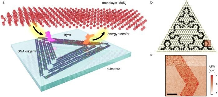
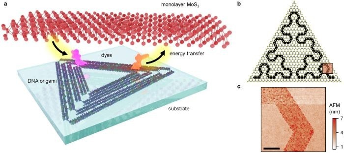
The layers of the obtained hybrid material are shown in (a), with a silicon dioxide substrate at the bottom, topped by a DNA origami structure (the triangle) carrying organic dye molecules (pink and orange blobs), which are close enough to the 2D molybdenum disulfide layer to exchange energy with it; (b) and (c) illustrate the DNA origami pattern. Image Credit: Shen Zhao et al./Small Methods

Originally inspired by graphene, a new class of atomically thin semiconductor materials – such as molybdenum disulfide – promises to enable electronic and optical devices that are smaller and more efficient than those achievable with conventional semiconductors like silicon. However, operating at such a small scale introduces a significant nanopatterning challenge: Creating well-defined, functional pathways within a two-dimensional material requires a level of precision that pushes the limits of current fabrication techniques.

“There are two basic approaches to creating a ‘landscape’ on a 2D semiconductor sheet to guide the conduction of excitons along preferred paths: Either you introduce some sort of defects that alter the initially uniform structure of the material, which is so far not possible to do with nanometer precision, or you deposit organic molecules on the monolayer, but until now it hasn’t been done in a controlled way, and the randomness of the resulting pattern puts a limitation on the device efficiency,” said study co-author Assistant Professor Irina Martynenko from Skoltech Physics.

See also  Scientists develop heat-activated protein control for targeted cell death

The team successfully demonstrated a way of depositing organic dye molecules on a monolayer of molybdenum disulfide using the technique of DNA origami. It involves designing DNA nanostructures approximately 100 nanometers in size that carry dye molecules at predefined positions. The resulting construct is placed on a chip and covered by a 2D semiconductor.
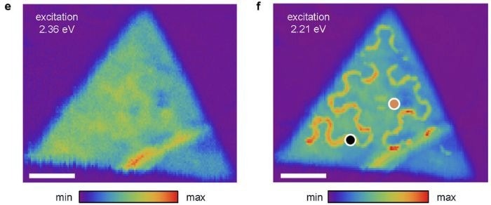
Image. Photoluminescence map of a triangular flake of atomically thin molybdenum disulfide with (right) and without (left) the underlying DNA origami-dye pattern’s contribution. The dye molecules carried by DNA clearly affect light emission across the flake. Credit: Shen Zhao et al./Small Methods

“Our experiments show that, firstly, the DNA origami-dye structures do assemble correctly and, second, the dye molecules and the molybdenum disulfide monolayer indeed exhibit the phenomenon of Förster resonance energy transfer. This is what enables the energy exchange between the two materials and therefore allows the semiconductor’s properties to be structured at the nanoscale by the deposited pattern. You can see this in photoluminescence images where a triangular molybdenum disulfide flake displays more or less uniform light emission at a wavelength not relevant for the dye molecules deposited behind the flake, but clearly emits more light in regions where the dye molecules absorb light,” said one of the study’s authors, Associate Professor Anvar Baimuratov from Skoltech Physics.

Now that the team has confirmed that DNA origami can be used to precisely and reliably pattern the energy landscape of two-dimensional semiconductors at the nanoscale, the researchers will attempt to create specific nanoelectronic and nanophotonic devices using this technique. Eventually, such nanostructured hybrid materials could enable the design of compact high-performance devices for optical computation and quantum simulations, light detection, etc.

See also  Scientists create nanofluidic chip with 'brain-like' memory pathways

Source link

DNA Marry materials Nanoelectronics Origami Scientists
Share. Facebook Twitter Pinterest LinkedIn Tumblr Email

Related Posts

Ultra-Large Spin Hall Oscillator Lattices Achieve Nanosecond Synchronization

September 1, 2026

DNA Nanotechnology May Open New Paths to Stroke Repair

August 31, 2026

Self-Heating Nanopores Turn Salt Precipitation Into Neuromorphic Memory

August 31, 2026

AI Searched 150 Million Materials – and Found Two Promising Candidates for Future Electronics

August 31, 2026
Add A Comment

Comments are closed.

Top Posts

Customizable nanomedicine platform shows promise for advancing personalized mRNA cancer therapeutics

October 30, 2025

Extra silver atom sparks 77-fold increase in Ag nanocluster photoluminescence quantum yield

October 14, 2025

Stretchable light-emitting material holds promise for photon-based devices

September 26, 2025

Subscribe to Updates

Get the latest sports news from SportsSite about soccer, football and tennis.

Explore the future with our Nanotech blog—covering innovations, research, applications, and breakthroughs shaping science, medicine, and modern technology.

We're social. Connect with us:

Facebook X (Twitter) Instagram YouTube
Top Insights

Biomass-Derived Nanomaterials Offer a Greener Route to Pollution Cleanup

September 1, 2026

Nanozyme Aptasensors Show Promise for Faster Food, Health, and Environmental Testing

September 1, 2026

Researchers Solve Two Major Problems Holding Back SiC Electronics

September 1, 2026

Subscribe to Updates

Get the latest creative news from FooBar about art, design and business.

  • Contact Us
  • Privacy Policy
  • Terms & Conditions

© 2026 elnano.com - All rights reserved.

Type above and press Enter to search. Press Esc to cancel.