
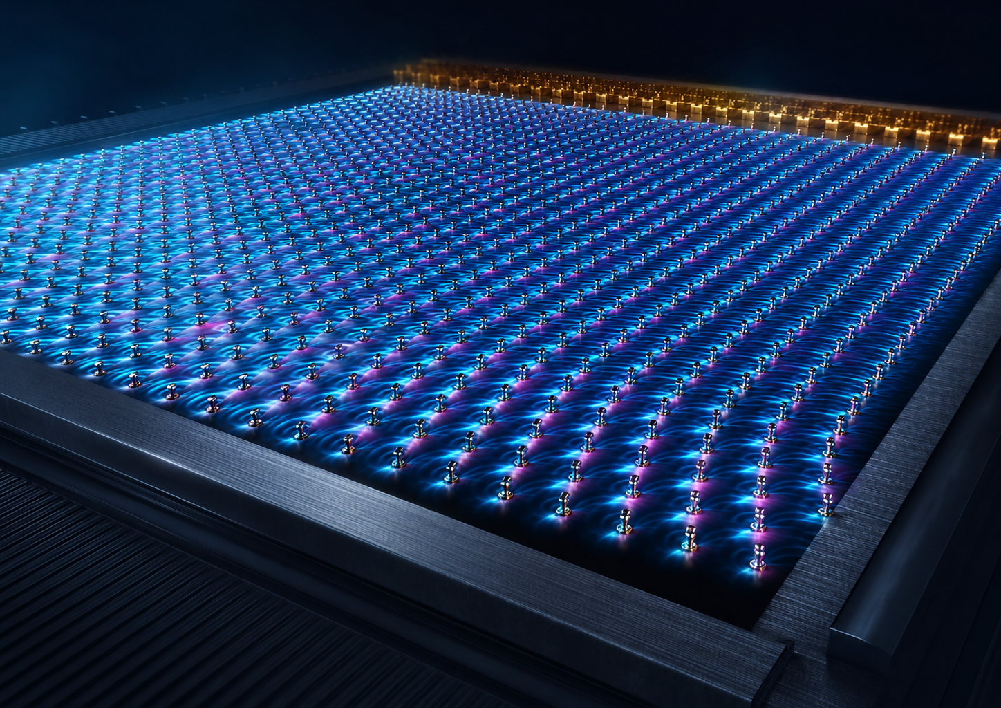
A 105,000-device spintronic lattice reaches global coherence within nanoseconds, setting a new scale for studying collective dynamics and future computing hardware.
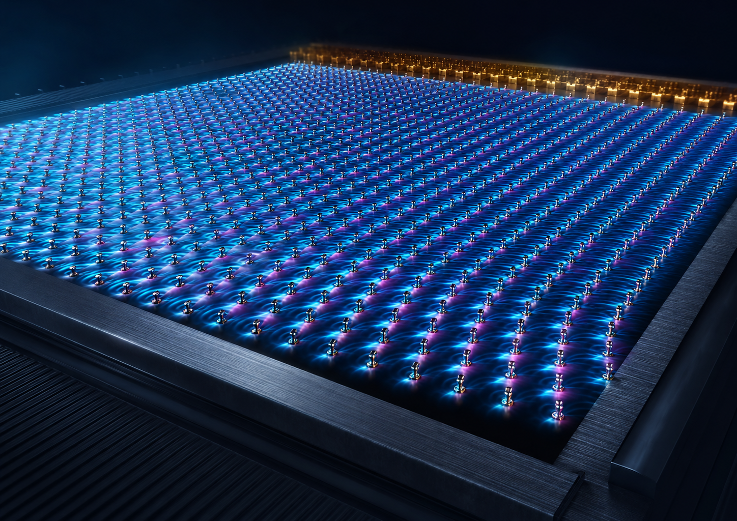
Paper: Nanosecond phase ordering in ultra-large spin Hall nano-oscillator lattices for unconventional computing. Image credit: AI-generated image created using ChatGPT/OpenAI
Magnonic and spin-wave-based technologies are being increasingly studied for unconventional computing and energy-efficient information processing. In this context, a paper recently published in the journal Nature Nanotechnology reported large-scale, fast synchronization in spin Hall nano-oscillator (SHNO) lattices containing up to N = 105,000 constrictions with 10–20 nm widths, with the largest lattice comprising 10-nm constrictions.
Synchronization in Large Oscillator Networks
Networks of coupled oscillators offer a versatile platform for implementing diverse physical-computing paradigms and for studying emergent collective dynamics. The phases of non-linear oscillators that interact through adjustable coupling spontaneously organize into coherent states that minimize an effective energy functional in suitable phase-reduced descriptions.
Such synchronization sheds light on the key features of non-equilibrium phase transitions and supports recent efforts to achieve analogue hardware for artificial intelligence, signal processing, and optimization. Among nanoscale oscillators, SHNOs are attractive due to their tunability, compatibility with complementary metal-oxide-semiconductor (CMOS) technology, and scalability.
SHNOs have been proposed as candidates for Ising-type optimization, as they generate microwave signals and synchronize with one another via spin waves driven by spin-orbit torques in heavy-metal/ferromagnet bilayers.
Yet, mutual synchronization has been restricted to arrays of 64 oscillators in previous demonstrations. Additionally, in larger networks, the real-time dynamics of phase ordering have not been thoroughly understood. In these networks, the collective behavior could develop on fundamentally different spatial and temporal scales.
The total number of mutually synchronized oscillators (N) is crucial from an applications perspective, as both coherence and microwave output power scale linearly with N, and very large interacting networks are required for sparse Ising-machine mappings to encode combinatorial problems that are practically relevant.
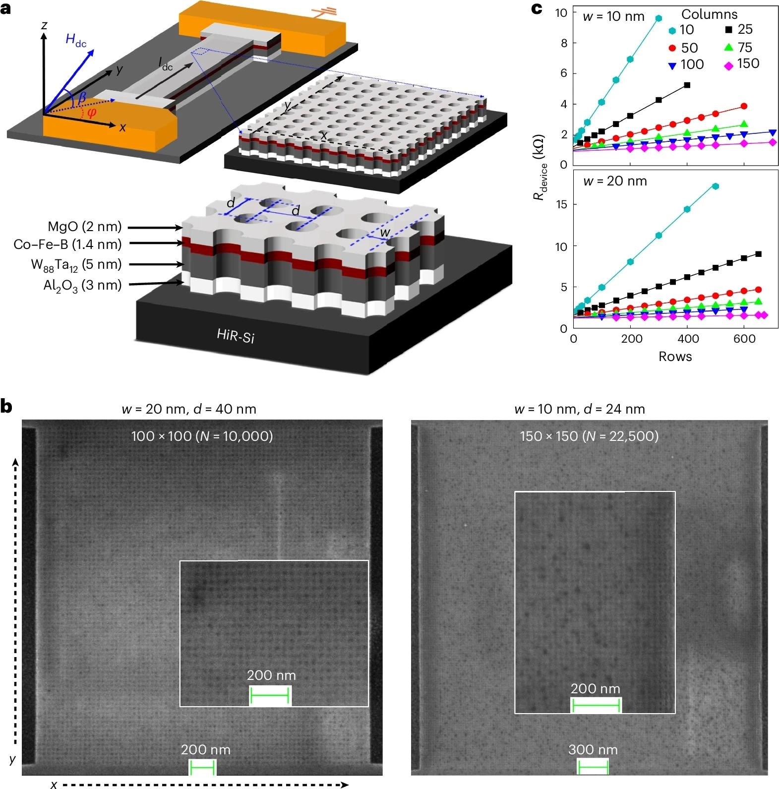
a, Schematic of the SHNO arrays and their material stack, showing consecutive zoom-ins. The top cartoon shows a small part of the thick Cu/Pt contact pads (orange), the remaining part of the mesa without any nanoconstrictions (light grey) and the actual nanoconstriction array (darker grey). The directions of the drive current and the applied field are indicated. The bottom cartoon shows the material stack and the nanoconstriction width (w) and centre-to-centre separation (d). b, SEM images of a 100 × 100 array made from 20-nm nanoconstrictions, and a 150 × 150 array made from 10-nm nanoconstrictions. c, Device resistance versus number of rows for different number of columns.
Nanosecond Phase Ordering in Ultra-large SHNOs
In this work, researchers demonstrated nanosecond phase ordering in lattices of up to N = 105,000 constriction-type SHNOs with widths of 10–20 nm.
They achieved this feat by combining three design strategies, including lower power dissipation through an energy-efficient tungsten–tantalum/cobalt–iron–boron (W–Ta/CoFeB) stack, reduction of interoscillator distance to a 24–40 nm pitch, and improved removal of heat by employing thermally conductive high-resistive silicon/aluminum oxide (HiR-Si/Al2O3) substrates.
Fabrication and Design of SHNO Arrays
Nanoconstriction SHNOs of 20 and 10 nm widths were fabricated using electron-beam lithography (EBL). Overall, 146 rectangular and square SHNO arrays with various numbers of rows (y = 10–1,000) and columns (x = 10–150) were defined in the center of 8 × 30 μm² mesas for the 20-nm SHNOs and 6 × 22 μm² mesas for the 10-nm SHNOs.
The center-to-center separation of the 20-nm SHNOs was d = 40 nm, and that of the 10-nm SHNOs was d = 24 nm. Researchers also fabricated three microbars (6 × 22, 6 × 18, and 6 × 12 μm²) between the SHNO arrays for characterization of spin-orbit torque using spin-torque ferromagnetic resonance (ST-FMR) measurements.
EBL was performed by first coating the material stack with negative resist, which was followed by EBL exposure. An Oxford Ionfab 300 Plus etcher was employed for argon-ion beam etching.
The ground–signal–ground (GSG) coplanar waveguides were defined using an optical lithography lift-off process on a sputter-deposited copper (Cu)/platinum (Pt) bilayer. The dimensions and quality of all arrays and SHNOs were inspected using scanning electron microscopy.
Subsequently, researchers performed electrical characterization and micro-Brillouin light scattering microscopy (μBLS) measurements. Moreover, time-resolved Brillouin light-scattering microscopy (TR-μBLS) measurements were performed on a few large-array SHNO devices to investigate the characteristic synchronization time.
Findings of the Study
Researchers successfully demonstrated mutual synchronization in SHNO lattices containing up to N = 105,000 nanoconstrictions, which extended the size of coherent SHNO networks by over three orders of magnitude.
The synchronized arrays showed linear scaling of microwave power with N and linewidth scaling as N–¹, yielding quality factors exceeding 106 and up to 9 nW output powers in the 20-nm devices, although these peak metrics were measured in different arrays.
Specifically, the combination of ultra-narrow linewidth and high output power may be relevant for microwave applications like ultrafast spectrum analysis and wireless communication.
TR-μBLS showed a weak, approximately logarithmic increase in synchronization time with array size. The synchronization time varied from 10 ns in arrays of 100 SHNOs to 45 ns for the largest lattices, consistent with Kuramoto-type collective phase-ordering dynamics in a large two-dimensional (2D) oscillator lattice.
Overall, all investigated arrays demonstrated well-defined single microwave signals consistent with complete mutual synchronization, although a few arrays showed multiple signals just above auto-oscillation onset, consistent with partial synchronization.
Further reductions in constriction spacing, engineering of alternative array geometries beyond the square lattice, and increases in magnetic thickness could enable larger, more functionally rich, and more strongly coupled networks.
In conclusion, although the present experiments did not implement programmable Ising couplings or explicit optimization tasks, the findings of this study demonstrate that spin-wave-mediated SHNO lattices are an experimentally accessible platform for studying collective oscillator physics and a basis for future embedded-Ising and reservoir-computing architectures operating at tens of gigahertz.