
Close Menu
  • News
    • Medical
    • Nanomaterials
    • AI & Robotics
    • 2D Materials
    • Metamaterials
    • Nanoelectronics
    • ETF’s
    • Medicine
  • Environment
    • Earth.com
    • TreeHugger
    • Nanomuscle
  • Beauty
    • Makeupanalysis
What's Hot

Biomass-Derived Nanomaterials Offer a Greener Route to Pollution Cleanup

September 1, 2026

Nanozyme Aptasensors Show Promise for Faster Food, Health, and Environmental Testing

September 1, 2026

Researchers Solve Two Major Problems Holding Back SiC Electronics

September 1, 2026
Facebook X (Twitter) Instagram
  • Contact Us
  • Privacy Policy
  • Terms & Conditions
Facebook X (Twitter) Instagram
Elnano – Global Innovative Nanotechnology SolutionsElnano – Global Innovative Nanotechnology Solutions
  • News
    • Medical
    • Nanomaterials
    • AI & Robotics
    • 2D Materials
    • Metamaterials
    • Nanoelectronics
    • ETF’s
    • Medicine
  • Environment
    • Earth.com
    • TreeHugger
    • Nanomuscle
  • Beauty
    • Makeupanalysis
Elnano – Global Innovative Nanotechnology SolutionsElnano – Global Innovative Nanotechnology Solutions
Home » Two-step method enables controllable WS₂ epitaxy growth
Nanotech

Two-step method enables controllable WS₂ epitaxy growth

September 24, 2025No Comments3 Mins Read
Share
Facebook Twitter LinkedIn Pinterest Email
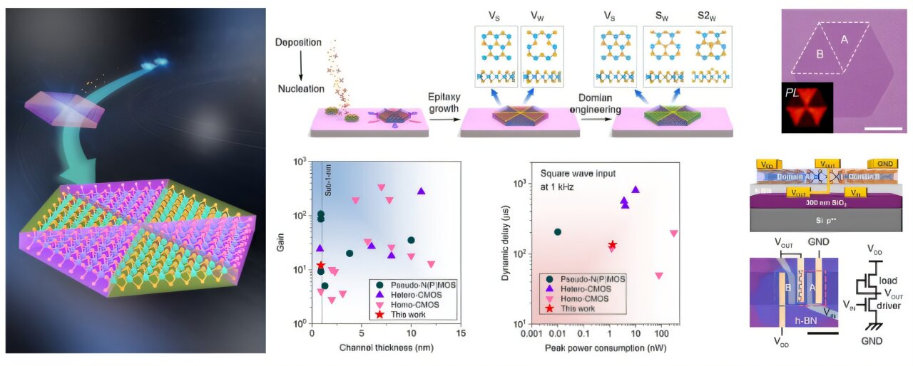
Two-step growth strategy for the WS2 homojunctions. (Image by USTC). Credit: USTC

In a study published in Journal of the American Chemical Society, a team led by Prof. Song Li from the University of Science and Technology of China (USTC) of the Chinese Academy of Sciences synthesized monolayer WS2 lateral homojunctions via in situ domain engineering, and enabled controllable direct chemical vapor deposition (CVD) growth of these structures.

Two-dimensional (2D) transition metal dichalcogenides are ideal candidates to replace silicon-based semiconductors due to their exceptional electrical properties at atomic scales. However, device applications require heterogeneous field-effect modulation behaviors across low-dimensional units. Van der Waals interactions or lateral atomic bonding allow damage-free integration into homojunctions/heterojunctions, but direct epitaxy growth remains challenging due to strict atomic species constraints.

In this study, researchers first determined optimal intrinsic defect configurations through theoretical simulations. Then they employed a two-step CVD method to achieve the in situ modulation of defect structures at the domain level, yielding homojunctions with tailored defect architectures.

In the first step, two types of domains in hexagonal samples were created under equilibrium growth conditions. In the second step, in order to meet the device requirements, the atomic configurations of specific domains were in situ manipulated to engineer the band structures of homojunctions.

It is worth mentioning that to control the epitaxy growth process, researchers manipulated the precursor feeding rates of tungsten trioxide and sulfur to an equilibrium state, which enabled the growth rate of the S-zigzag edges to be equal to that of the W-zigzag edges.

The synthesized WS2 homojunctions exhibited distinct field-effect characteristics while maintaining atomic lattice matching and customized band alignment at interfaces. Logic inverters based on these structures demonstrated rail-to-rail operation with a peak voltage gain of 12, dynamic delay of ~135 μs, and ultralow power consumption of 1.3 nW.

See also  Nanoparticles That Boost Tomato Plant Growth

The study provides a new perspective on in-situ engineering of both defect configurations and distributions within atomic layers, and a more comprehensive understanding of 2D landscape.

More information:
Qilong Cui et al, Growth of Monolayer WS2 Lateral Homojunctions via In Situ Domain Engineering, Journal of the American Chemical Society (2025). DOI: 10.1021/jacs.5c04546

Provided by
University of Science and Technology of China


Citation:
Two-step method enables controllable WS₂ epitaxy growth (2025, September 23)
retrieved 24 September 2025
from https://phys.org/news/2025-09-method-enables-ws8322-epitaxy-growth.html

This document is subject to copyright. Apart from any fair dealing for the purpose of private study or research, no
part may be reproduced without the written permission. The content is provided for information purposes only.


Source link

controllable enables epitaxy Growth Method Twostep WS₂
Share. Facebook Twitter Pinterest LinkedIn Tumblr Email

Related Posts

New Versatile Nanoplatelet Platform Optimizes Tumor Imaging and Cancer Destruction

September 1, 2026

IBM debuts world’s first sub-1 nanometre chip technology

August 31, 2026

Atom-by-atom manufacturing takes a step forward

August 31, 2026

Pittcon Announces 2025 Nobel Laureate, Dr. Omar Yaghi, as Wallace H. Coulter Keynote Lecturer

August 31, 2026
Add A Comment

Comments are closed.

Top Posts

Twisted Graphene Shows Unconventional Superconductivity

November 7, 2025

Nanoparticles supercharge vinegar’s old-fashioned wound healing power

September 22, 2025

Nanoscale Gold Detects Ovarian Cancer Markers in Bodily Fluids

September 19, 2025

Subscribe to Updates

Get the latest sports news from SportsSite about soccer, football and tennis.

Explore the future with our Nanotech blog—covering innovations, research, applications, and breakthroughs shaping science, medicine, and modern technology.

We're social. Connect with us:

Facebook X (Twitter) Instagram YouTube
Top Insights

Biomass-Derived Nanomaterials Offer a Greener Route to Pollution Cleanup

September 1, 2026

Nanozyme Aptasensors Show Promise for Faster Food, Health, and Environmental Testing

September 1, 2026

Researchers Solve Two Major Problems Holding Back SiC Electronics

September 1, 2026

Subscribe to Updates

Get the latest creative news from FooBar about art, design and business.

  • Contact Us
  • Privacy Policy
  • Terms & Conditions

© 2026 elnano.com - All rights reserved.

Type above and press Enter to search. Press Esc to cancel.