
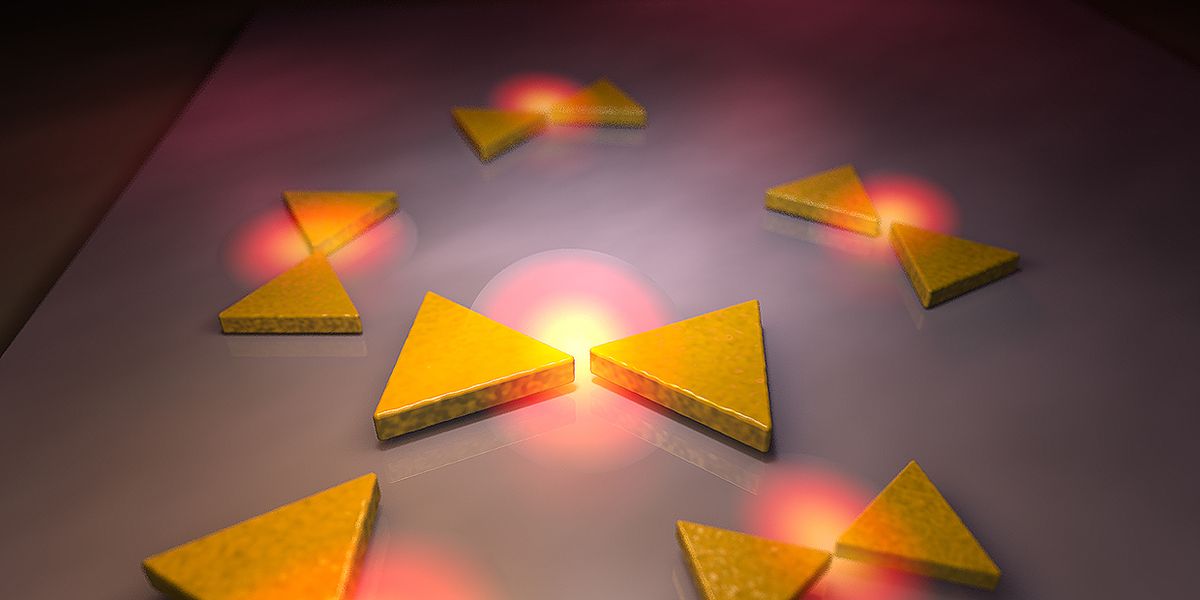
This graphic shows how DNA origami shapes are transformed into metallic nanostructures in a new process.Illustration: M. Kostiainen and V. Linko
To combine these two technologies, the scientists started with DNA origami structures, which are essentially DNA strands that have been folded into chosen shapes, and deposited them on a substrate that has a sacrificial silicon layer on top of it.
After this step, a silicon oxide is grown on the silicon layer. The trick is that the silicon oxide does not grow on top of the DNA origami structures and as a result leaves origami-shaped openings in the oxide layer.
“This is exactly the critical step within the process that ties up the otherwise seemingly disparate techniques, since from this step on, the silicon oxide layer is used as a hard mask for more standard fabrication steps just like in a conventional lithography,” said Toppari.
In the final step of the process, metal is evaporated through these openings on the uncovered substrate and all the redundant sacrificial layers are removed during the lift off. This leaves only the metallic nanostructures having the original origami-shape on the substrate.
“In a sense the role of the origami is to replace the slow, focused ion beam writing or inaccurate UV light exposure used for patterning the resist,” said Toppari.
The clear benefits of this approach are that the DNA origami has superior spatial accuracy, according to Toppari. Also, the shape and size of the structures have many plasmonic properties at the visible wavelength range that have only been possible to achieve in infrared range previously. Plasmonics involves the exploitation of surface plasmons that are generated when photons hit a metal structure to reduce the size of wavelengths of light.
Another advantage of this approach, according to Toppari, is that the method is highly parallel, so one could conceivably create millions of these tiny metal shapes in one go. This stands in stark contrast to to e-beam lithography where each structure has to be drawn one by one.
“The only limitations of our method are that it is a surface-based technique, meaning that one cannot create colloid dispersions of metal nanostructures. And organization of the structures on the substrate, for example, to form a regular lattice, is not possible so far,” said Toppari.
There are many potential applications capable of utilizing DALI, according to Toppari. For example, better surfaces and structures for Surface-enhanced Raman spectroscopy (SERS) and biosensing could be easily fabricated allowing for the efficient detection of really low amounts of material.
Also, as the DNA origami is fully programmable, it would be possible to use different shapes to tailor the optical properties of the substrates. This opens up many new possibilities, according to Toppari, such as fluorescence enhancement for optical surfaces and even to fabricate metamaterials operating at visible range that have surfaces with a negative refractive index.
The method is also fully compatible with all the standard semiconductor fabrication processes after the formation of the silicon oxide layer, according to Toppari.
Toppari added: “The only extra engineering needed would be the origami fabrication and immobilization on the surface which, on the other hand, are standard processes in chemical industry. All in all, as the method combines bottom-up and top-down fabrication, its commercial implementation would as well combine semiconductor and chemical industry processes.”