Close Menu
  • News
    • Medical
    • Nanomaterials
    • AI & Robotics
    • 2D Materials
    • Metamaterials
    • Nanoelectronics
    • ETF’s
    • Medicine
  • Environment
    • Earth.com
    • TreeHugger
    • Nanomuscle
  • Beauty
    • Makeupanalysis
What's Hot

NY Creates Begins Installation of First Major Tool for High NA EUV Lithography Center at Albany Nanotech Complex

May 7, 2026

Orange Leaf Extract Produces Greener Antibacterial Nanoparticles

April 9, 2026

Pittcon’s First San Antonio Experience a Roaring Success

April 8, 2026
Facebook X (Twitter) Instagram
  • Contact Us
  • Privacy Policy
  • Terms & Conditions
Facebook X (Twitter) Instagram
Elnano – Global Innovative Nanotechnology SolutionsElnano – Global Innovative Nanotechnology Solutions
  • News
    • Medical
    • Nanomaterials
    • AI & Robotics
    • 2D Materials
    • Metamaterials
    • Nanoelectronics
    • ETF’s
    • Medicine
  • Environment
    • Earth.com
    • TreeHugger
    • Nanomuscle
  • Beauty
    • Makeupanalysis
Elnano – Global Innovative Nanotechnology SolutionsElnano – Global Innovative Nanotechnology Solutions
Home » 39.5 mm for High Precision
Nanomaterials

39.5 mm for High Precision

September 20, 2025No Comments2 Mins Read
Share
Facebook Twitter LinkedIn Pinterest Email

Unique single-module 3-axis precision motion platform.

Ultra-low profile 3-axis nanopositioning stage is less than 40 mm tall. Image Credit: PI (Physik Instrumente) LP

PI (Physik Instrumente), a leader in precision motion control, has introduced the A-361 air-bearing XY-rotation stage, a compact nanopositioning platform engineered for ultra-high precision and stability in demanding research and industrial applications.

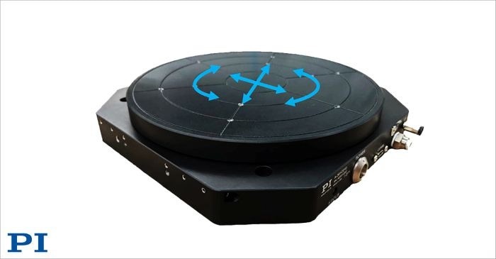
The A-361 XY-rotation stage combines an exceptionally low profile of just 39.5 mm with a generous 200 mm diameter motion platform. It provides translational motion of 5 mm in both X and Y, along with rotational motion around the Z axis of 2°.

Applications

The A-361 PIglide XY-theta stage is particularly well suited for wafer inspection, flat-panel display metrology, fiber and optics alignment, maskless lithography, and µLED manufacturing. Its clean, non-contact design, combined with ultra-high stability and resolution, make it a compelling solution for semiconductor and photonics production environments.

Frictionless Bearing Design, Lock-Down Mechanism for Ultra-High Stability

With its frictionless air bearings and non-contact motors, the A-361 ensures smooth motion without wear, enabling virtually maintenance-free operation and a service life measured in decades. Integrated position-locking further enhances stability, eliminating servo jitter in critical measurement and alignment tasks. A built-in vacuum chuck accommodates wafers or other delicate substrates, making the stage well suited for semiconductor and optics applications.

Frictionless Direct Drives, High Dynamics

Voice-coil direct drives provide frictionless, highly dynamic response, generating up to 6 N of continuous force and 19.2 N peak. Despite its compact footprint, the A-361 supports payloads up to 3 kg, and its lightweight design with hard-anodized aluminum construction ensures stability and durability.

Designed for cleanroom operation, the A-361 requires only dry, oil-free compressed air in accordance with ISO 8573-1 purity standards. Air consumption is limited to 28 L/min, making the system highly efficient for continuous operation. When combined with the A-523 Z Tip/Tilt Stage, the A-361 forms the basis of a versatile six-degree-of-freedom nanopositioning stack, enabling complete spatial control for precision alignment tasks in photonics, optics, and micro-assembly. Complementing the platform, PI provides integrated accessories such as air-preparation kits, multi-axis controllers, and custom cabling solutions, ensuring seamless system integration and enhanced performance.

See also  PI Introduces Versatile Modular Precision Linear Stages

Industries Served

Semiconductor test and wafer inspection, photonics and fiber alignment, precision optics alignment, flat panel inspection, maskless lithography, advanced LED manufacturing, tribology, material research.

Source:

PI (Physik Instrumente) LP

Source link

High precision
Share. Facebook Twitter Pinterest LinkedIn Tumblr Email

Related Posts

NY Creates Begins Installation of First Major Tool for High NA EUV Lithography Center at Albany Nanotech Complex

May 7, 2026

Ultrafast Electron Microscopy Captures the Intricate Dynamics of Plasmonic Nanostructures

April 7, 2026

Researchers Call for Help with Reproducibility Crisis

April 6, 2026

6-Channel Piezo Driver for Precision Actuators & Transducers

April 6, 2026
Add A Comment

Comments are closed.

Top Posts

Developing Albumin-Recruiting Nanoparticle for mRNA Vaccines

October 16, 2025

Johns Hopkins Unlocks New Chemistry for Faster, Smaller Microchips

September 25, 2025

A reusable, washable nanofiber membrane can filter water sustainably

October 24, 2025

Subscribe to Updates

Get the latest sports news from SportsSite about soccer, football and tennis.

Explore the future with our Nanotech blog—covering innovations, research, applications, and breakthroughs shaping science, medicine, and modern technology.

We're social. Connect with us:

Facebook X (Twitter) Instagram YouTube
Top Insights

NY Creates Begins Installation of First Major Tool for High NA EUV Lithography Center at Albany Nanotech Complex

May 7, 2026

Orange Leaf Extract Produces Greener Antibacterial Nanoparticles

April 9, 2026

Pittcon’s First San Antonio Experience a Roaring Success

April 8, 2026

Subscribe to Updates

Get the latest creative news from FooBar about art, design and business.

  • Contact Us
  • Privacy Policy
  • Terms & Conditions

© 2026 elnano.com - All rights reserved.

Type above and press Enter to search. Press Esc to cancel.