
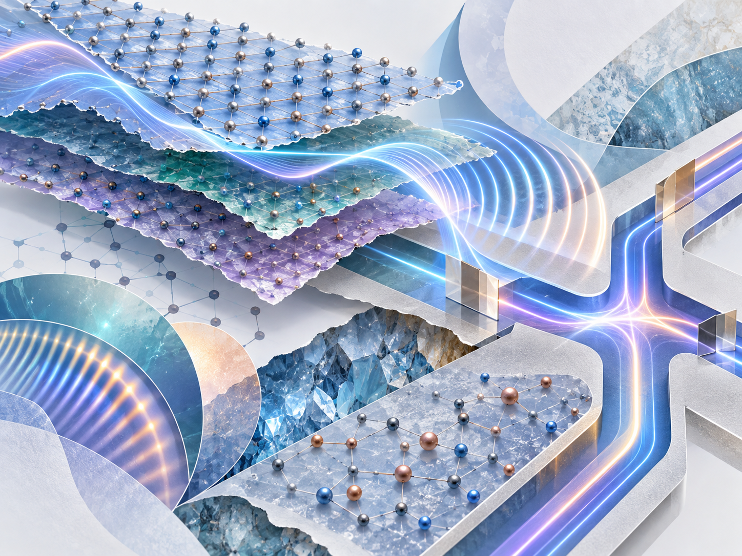
A wide-ranging review examines how crystal symmetry, nanoscale fabrication, and polariton behavior could shape a new class of compact photonic devices.
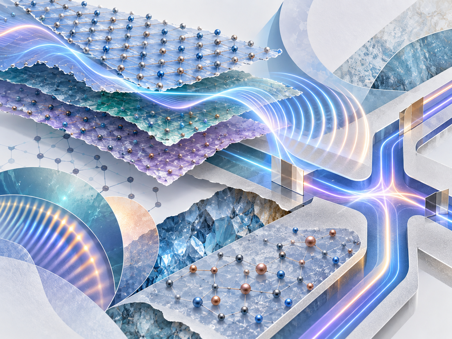
Review: Two-dimensional metal oxide polaritonics. AI-generated abstract conceptual image created using ChatGPT/OpenAI
Two-dimensional (2D) metal oxides (MOs) play a key role in energy applications and semiconductor optoelectronics. Recently, anisotropic and ultra-confined polaritons in 2D MOs have sparked renewed interest in nanophotonics. A paper recently published in the journal Nature Communications reviewed strategies for synthesizing and manipulating 2D polaritonic MOs and proposed device architectures that exploit their unusual optical properties.
Metal Interface Oxidation
The metal interface oxidation approach enables the fabrication of 2D materials through oxidation reactions precisely controlled at the environment–metal surface interface. In the polished-metal oxidation method, transfer printing, atmospheric control, and surface polishing are used to prepare atomic-thickness oxides such as titanium dioxide.
While this method shows good compatibility with various metals, it predominantly yields hexagonal crystal structures, thereby limiting the symmetry diversity crucial for rich polaritonic dispersion.
In the liquid metal interface approach, gallium-based alloys are employed, which spontaneously oxidize to form ultrathin oxide layers in oxygen-containing environments. This process can produce single crystals and heterostructures by combining the benefits of vapor-phase synthesis and mechanical exfoliation.
The derived bubble-assisted strategy allows suspension drop-casting and has also been extended to liquid metal printing. With lateral dimensions spanning tens of micrometers while retaining atomic-level thickness, it could support highly confined polaritons in integrated devices.
Yet material compatibility and crystallinity are key bottlenecks limiting the practical application of this method.
Mechanical Exfoliation
2D nanosheets are fabricated using this approach by iteratively peeling the bulk material, enabling the preparation of high-quality single crystals such as α-molybdenum trioxide (α-MoO3).
While mechanical exfoliation is a simple method for obtaining high-quality, clean crystals, its poor reproducibility, including batch variations, uncontrollable sizes and thicknesses, and low yields, limits large-scale production. Still, mechanical exfoliation remains a reliable choice for fundamental polariton research.
The solvent exfoliation method has been developed for non-layered MOs. While this strategy can support larger-scale MO preparation, compositional alterations, structural defects, and solvent residues hinder its application in polariton research.
Vapor-Phase Deposition
A separate bottom-up route is vapor-phase deposition. Chemical vapor deposition can produce high-quality ultrathin nanosheets, while atomic layer deposition provides atomic-level thickness control. Reproducibility and simple, large-area preparation still need improvement.
Wet Chemical Synthesis
Wet chemical synthesis, a template-confined approach for preparing nanomaterials, is categorized into hard-template and soft-template methods. In the soft-template method, surfactant micelles serve as templates to guide confined MO growth in 2D, thereby producing nanosheets.
Soft-template synthesis can produce 2D MOs at a large scale with uniform size and controllable morphology. Yet, their utilization in polariton studies is hampered by low crystallinity, poor batch-to-batch reproducibility, and surfactant residues.
In hard-template synthesis, physical barriers such as salt crystals, graphene, or hexagonal boron nitride (hBN) guide growth within confined spaces, producing various 2D MO nanosheets, such as MoO3.
While this strategy offers high yields and simple operation, surface heterogeneity, significant size variations, and morphological irregularities complicate its application in polariton studies.
Photonic Computing with Polaritons
Optical computing combines high-speed operation with frequency multiplexing and spatial parallelism for advanced information processing. Here, the authors proposed an α-MoO3/graphene heterostructure-based NAND logic gate that uses in-plane phonon polariton (PhP) focusing and electrical gating.
In the proposed design, scanning near-field microscopy would read the amplitude information and output the phase. This design exploits the focusing effect in the graphene-hybrid structure, induced by negative refraction, and the unique propagation modes of the various Reststrahlen bands (RBs) in α-MoO3.
The authors defined the incident light within the RB1, RB2, and RB3 bands as input signals. The output amplitude depends on whether phase cancellation of the in-plane wavevectors occurs. With all three signals present, phase cancellation at both focal points produces a “0” output; if any signal is absent, cancellation fails at least at one focal point, producing a “1” output.
Controlling the in-plane wavevectors in various RBs remains a key challenge. This in-plane-tunable, anisotropic MO-based NAND gate holds significant promise for on-chip photonic computing.
Phase-change Polariton Waveguides
Controllable guiding of electromagnetic waves is crucial in integrated photonics and nano-optics. In this work, the authors proposed a design for a programmable polariton waveguide using spatially controlled crystallinity within a phase-change MO.
Crystalline domains, unlike amorphous regions, support propagation of PhPs. These crystalline regions can guide collimated polaritons within an amorphous flake along predefined channels.
The proposed waveguide could be reconfigured reversibly using localized annealing, tip-induced hydrogen intercalation, or ultrafast laser writing, allowing repeated erasing and writing of guiding paths.
The controllable thickness of the 2D crystalline layer governs optical-field confinement. The precision of crystallization-induced fabrication and the inhomogeneity of crystalline channels are the major challenges for realizing such a design. Amorphous-crystalline grain boundaries would also introduce losses, potentially reducing crosstalk between adjacent channels under steady-state excitation.
The proposed waveguide could support reconfigurable nanophotonic circuits by combining long-range energy transport, the strong field confinement of MOs, and the propagation features of crystalline layers.
The authors conclude that the rapid advances in 2D MO polaritonics could stimulate further work on advanced on-chip photonic systems. They also stress that the field remains in its infancy, with practical use requiring better control of synthesis, the trade-off between confinement and propagation length, and symmetry-breaking effects.