
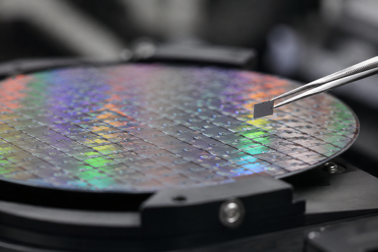
A carbon film less than a nanometer thick combines unusual electrical, mechanical, and barrier properties that could address some of the toughest challenges facing increasingly compact electronic devices.
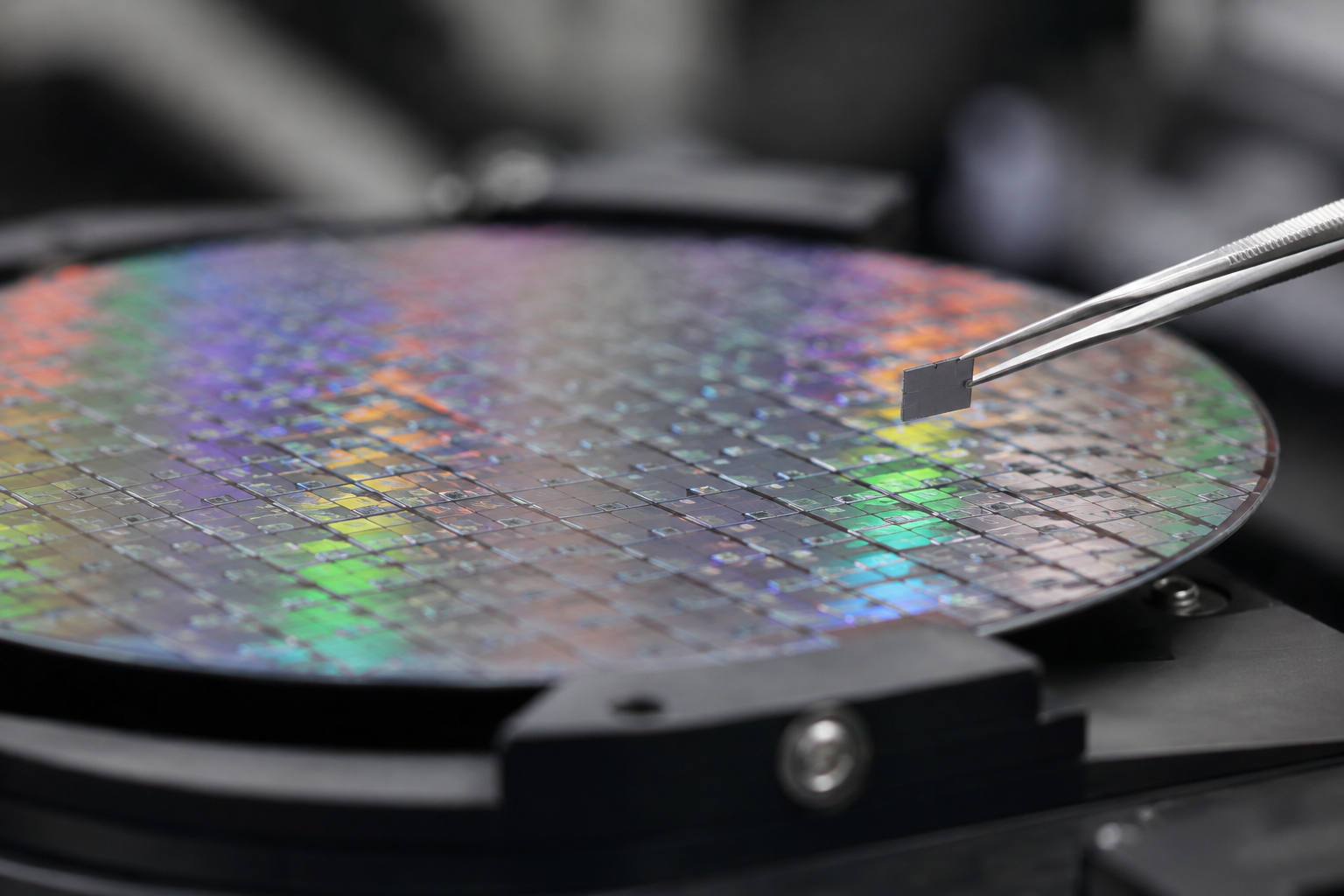
Paper: Atomically thin amorphous carbon with an ultralow dielectric constant. AI-generated conceptual image created using ChatGPT/OpenAI
In a recent research article published in the journal Nature Electronics, researchers demonstrated that atomically thin amorphous carbon films can function as mechanically robust ultralow-k dielectrics with a dielectric constant of 1.35 and an effective barrier to metal-ion diffusion, potentially supporting further scaling of integrated circuits and 2D electronics.
Ultralow-k Scaling Needs
As electronic devices become smaller and more complex, finding suitable insulating materials is becoming increasingly difficult. This is especially important as two-dimensional (2D) materials are introduced into microelectronics.
When the spacing between conductors falls below 10 nanometers, unwanted capacitance can significantly affect device performance. Conventional low-k dielectrics are not well suited to these dimensions. At very small thicknesses, porous materials can lose mechanical strength and perform poorly as metal-ion diffusion barriers, while other low-k dielectrics can lose their favorable properties as their thickness changes.
These limitations create a clear need for atomically thin materials with an ultralow dielectric constant that can remain stable and effective even at only a few atomic layers. Developing such materials could help extend the scaling of CMOS technology while also supporting increasingly complex device designs, including three-dimensional transistor architectures.
ULK Carbon Synthesis & Characterization
To overcome these limitations, the researchers developed a low-temperature chemical vapor deposition”>CVD process for growing atomically thin amorphous carbon films. Acetylene and argon were introduced at a 1:2 ratio under low pressure, while an excimer laser and remote plasma source assisted film growth. Depending on the substrate and device structure, either direct or indirect laser exposure was used, with processing temperatures maintained at 250–300 °C.
The resulting films, ranging from approximately 0.8 to 2.7 nm in thickness, were examined using AFM and cross-sectional TEM. Atomic-resolution STEM and SAED confirmed their disordered, amorphous structure, while X-ray photoelectron spectroscopy”>XPS and Raman spectroscopy provided information on chemical composition and carbon bonding, showing that the films were predominantly sp²-hybridized carbon. The process also enabled wafer-scale, substrate-independent, and conformal growth with controllable thickness.
Electrical performance was studied using MIM capacitors. Capacitance measurements were used to determine the dielectric constant, while voltage sweeps and conductive AFM were used to evaluate dielectric breakdown and leakage current. Weibull analysis was used to assess reliability. Copper diffusion resistance was investigated using dedicated capacitor structures and time-dependent dielectric breakdown measurements. Finally, spectroscopic ellipsometry was used to determine optical permittivity and estimate the optical band gap.
ULK Properties & Reliability
The study showed that atomically thin amorphous carbon has several properties that make it a strong candidate for ultralow-k dielectrics in future electronic devices. Most importantly, the films achieved a dielectric constant of just 1.35 ± 0.10 across the measured thickness range, which remained consistent even when the thickness was reduced to 0.8 nm. At this subnanometer thickness, where electrons can tunnel directly through such an extremely thin layer, complicating conventional measurements, a bilayer device and circuit model produced a consistent value of 1.35 ± 0.34. This is particularly significant because crystalline hBN has a substantially higher dielectric constant, amorphous boron nitride shows optimal ultralow-k performance around 3 nm, and porous covalent organic frameworks are mechanically weak and difficult to scale below about 20 nm.
The unusually low dielectric constant was attributed to the material’s amorphous, sp²-rich structure, nonpolar carbon-carbon bonds, and low density, all of which reduce its polarizability. Structural disorder also localizes electronic states, limiting the formation of electrical dipoles. Despite its predominantly sp² bonding, the film remained highly insulating, with an optical band gap of about 2.4 eV.
The films also performed well under high electric fields. Their dielectric strength reached 28 MV cm–¹ in MIM capacitor measurements and 31 MV cm–¹ using conductive AFM. Weibull slopes above 4 indicated relatively consistent breakdown behavior across the tested devices. Leakage current also decreased as the films became thicker, with films of 1.4 nm or more meeting low-power leakage requirements for transistor applications. Nanoindentation also indicated a hardness of around 100 GPa.
Another important result was their ability to block copper diffusion. Even a 0.8 nm carbon layer provided strong resistance to copper-ion migration. Time-dependent dielectric breakdown measurements were used to project a time to failure exceeding 10¹0 seconds at 50% probability at an operating field of 0.5 MV cm–¹. The projected performance was reported to exceed conventional TaN and several recently investigated diffusion barriers by at least two orders of magnitude.
These results are especially encouraging from a manufacturing perspective. Microscopy showed that 1.4 nm films could continuously coat trench sidewalls, bottoms, and patterned metal structures. The films combine a very low dielectric constant, high breakdown strength, and effective resistance to copper diffusion within a single ultrathin layer. Since they can also be grown below 300 °C with controlled thickness and conformal coverage, the authors argue that the process is promising for practical CMOS implementation.
Outlook for CMOS Scaling
In summary, this research introduces an atomically thin amorphous carbon material that embodies a unique combination of highly desirable properties, making it a promising candidate for next-generation nanoelectronic applications.
Its ultralow dielectric constant of 1.35, maintained even at 0.8 nm thickness, addresses a critical need to reduce parasitic capacitance in highly scaled circuits. Coupled with its high dielectric strength (28–31 MV cm–¹), mechanical hardness, and strong projected effectiveness as a metal-ion-diffusion barrier, even at atomic thicknesses, this material presents a potential solution to fundamental limitations faced by current dielectric technologies.
The low-temperature, direct, and conformal growth process, alongside its thickness-independent dielectric constant, significantly improves its prospects for practical implementation in semiconductor manufacturing. This multifunctional ULK carbon could support continued CMOS scaling and open possibilities for advanced beyond-CMOS 2D electronics, potentially simplifying complex interconnect stacks in 3D devices and enhancing overall device performance.