

The latest review of 2D materials investigates how they could extend Moore’s Law, surpass silicon’s limits, and enable flexible, low-power, next-generation electronics, from AI chips to wearable devices.
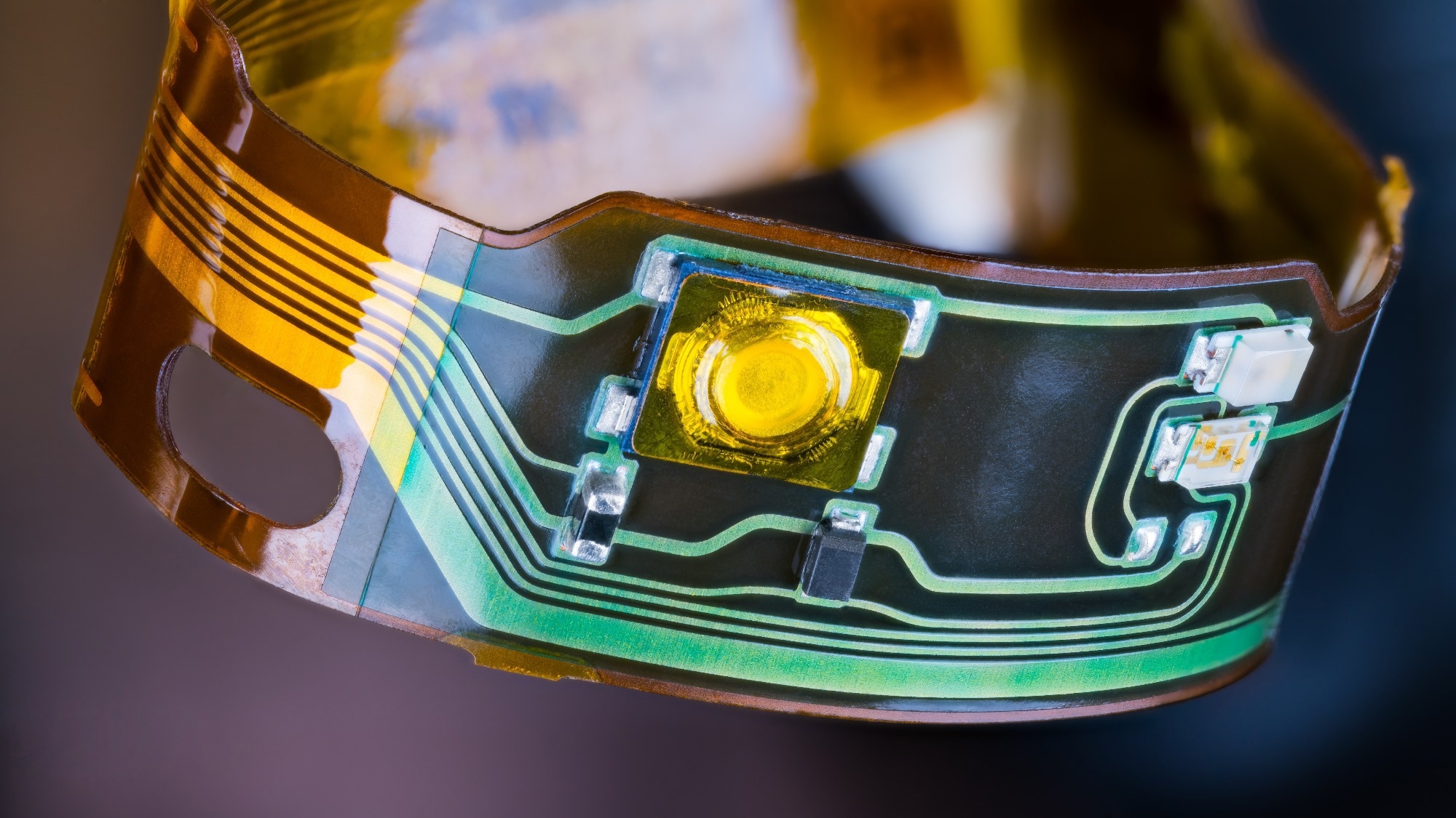
Image Credit: KPixMining/Shutterstock.com
A new review in Nano-Micro Letters explores how two-dimensional (2D) materials could reshape the future of electronics and integrated circuits. The paper demonstrates their promise in overcoming the constraints of traditional silicon semiconductors and sustaining progress in the post-Moore era.
Why This Research Matters
As semiconductor manufacturing approaches sub-10 nm technology nodes, classic bulk semiconductors (often Si-based) struggle with reduced carrier mobility and rising power consumption. 2D materials, just a few atoms thick and with distinct electrical characteristics, retain high mobility even at sub-nanometre scales, offering a way around these bottlenecks.
Modern demands extend well beyond faster processors. Emerging technologies like 5G/6G networks, artificial intelligence, and neuromorphic systems require more adaptable and multifunctional components.
2D materials could underpin flexible sensors, advanced in-memory computing, and wearable electronics designed for these use cases with their unique properties.
Innovative Design and Mechanisms
The study thoroughly examines a variety of 2D materials, including transition metal dichalcogenides, black phosphorus, hexagonal boron nitride, and graphene. These materials have a wide range of electronic characteristics, including as insulators, semiconductors, and metals. Their diversity makes them applicable in a variety of applications.
2D materials can be engineered to form advanced device architectures, such as tunnel field-effect transistors, negative capacitance field-effect transistors, and impact-ionization FETs.
The review assessed these devices based on their steep subthreshold slopes and high on/off ratios, which result in much lower power consumption and improved performance compared to typical silicon-based devices.
Research shows that 2D materials have huge potential for 3D monolithic integration, which allows for the creation of high-density, low-power integrated circuits. Their mechanical flexibility and resilience also make them perfect for flexible and wearable electronics, creating new opportunities in healthcare, IoT, and consumer electronics.
Applications
2D material-based memristors and memtransistors show great promise for in-memory computing and neuromorphic applications. These devices could be used to conduct logic operations and data storage simultaneously, resulting in lower latency and power consumption than standard von Neumann systems.
The study looks at a variety of small and large-scale integrated circuits made of 2D materials, such as inverters, logic gates, and memory arrays. These circuits show remarkable performance, with high gain, low power consumption, and outstanding stability, opening the way for future high-speed computing applications.
Future Outlook
The authors call for further work on improving the synthesis and scalability of 2D materials, refining device designs, and developing manufacturing techniques. They also emphasize the need to integrate 2D materials with existing silicon technologies to bring these innovations to market.
By examining their unique properties, inventive device designs, and wide-ranging applications of 2D materials, this review makes a compelling case for their role in overcoming the limitations of traditional semiconductors and in the future of computer technologies.
Journal Reference:
Qin, L. and Wang, L. (2025) Two-Dimensional Materials, the Ultimate Solution for Future Electronics and Very-Large-Scale Integrated Circuits. Nano-Micro Letters. doi.org/10.1007/s40820-025-01769-2.
Source: