
IBM debuts world’s first sub-1 nanometre chip technology
IBM has unveiled a 0.7 nm chip architecture that stacks transistors in three dimensions, extending semiconductor scaling into the angstrom era and promising major gains in performance and energy efficiency.
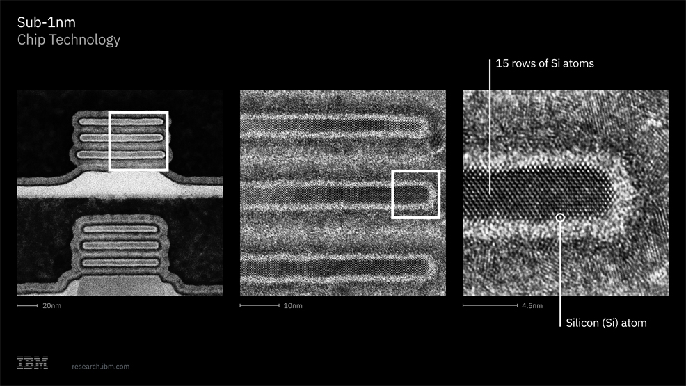
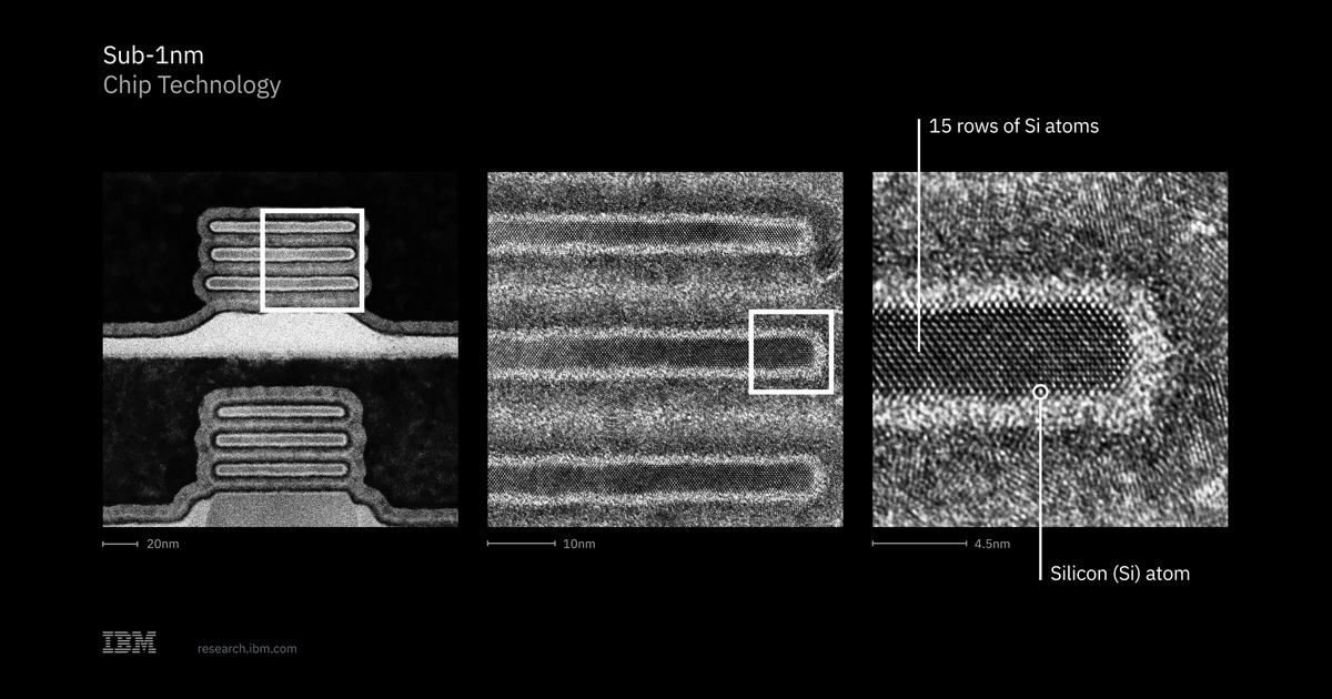
Computing giant IBM has unveiled a major semiconductor breakthrough with the introduction of the world’s first sub-1 nanometre (nm) class of chip technology, featuring a revolutionary transistor architecture at the 0.7 nm, or 7 angstrom node. The achievement marks a landmark moment for an industry facing the physical limits of traditional chip scaling. Semiconductors play critical roles in everything from computing, to appliances, to communication devices, transportation systems, and critical infrastructure.
The new chip packs nearly 100 billion transistors onto an area the size of a fingernail, nearly twice the density of IBM’s 2 nm chip, which the company unveiled back in May 2021.
Enabled by a series of structural and material innovations – including IBM’s groundbreaking three-dimensional “nanostack” architecture – the technology demonstrates how continued gains in performance and efficiency remain possible even as chip features approach atomic dimensions.
Published technical results suggest the new chip technology could offer a substantial leap in capability – up to 50% more performance, or 70% greater energy efficiency than IBM’s previous generation of node chips – supercharging compute for applications ranging from generative AI and cloud infrastructure to everyday consumer electronic devices.

“IBM’s latest chip breakthrough marks a landmark moment in computing, pushing technology beyond the nanometre era to the scale of atoms. With our new nanostack architecture, we’re not just making smaller transistors, we’re reinventing how chips are built to deliver dramatically more power and energy efficiency,” said Jay Gambetta, Director of IBM Research. “This industry-first innovation continues IBM’s legacy of leading in next-generation technologies and sets the foundation for the next era of computing.”
Nanostack is the industry’s first known three-dimensional, nanosheet-based design. It represents a major advance beyond nanosheet technology, with a design that vertically stacks and staggers transistors, taking advantage of 3D sequential integration to pack more transistors onto a chip. The design also unlocks the use of different material combinations within each stacked layer, optimising performance and power efficiency of each transistor independent of the other.
In new research presented at the recent VLSI Symposium, IBM researchers also demonstrated that nanostack can deliver a 40% improvement in the scaling of static random-access memory (SRAM). This type of memory sits directly on the chip, close to the logic circuits, allowing processors to access data much faster than if they had to keep reaching out to separate memory components. For AI systems, which constantly move huge amounts of data between memory and processing units, denser SRAM could therefore make chips faster and more energy efficient.
“It’s a massive leap in memory capacity – the likes of which the industry hasn’t seen in over a decade,” IBM wrote in a blog post. “Accessing on-chip memory is one of the key bottlenecks in AI computing that our team has addressed.”
IBM says its breakthrough opens a new route for chip scaling into the 2030s and beyond. By moving from conventional 2D shrinking to 3D stacking, the company believes nanostack could support another 10 to 15 years of progress in semiconductor performance, density, and efficiency.
Comments »
If you enjoyed this article, please consider sharing it: