

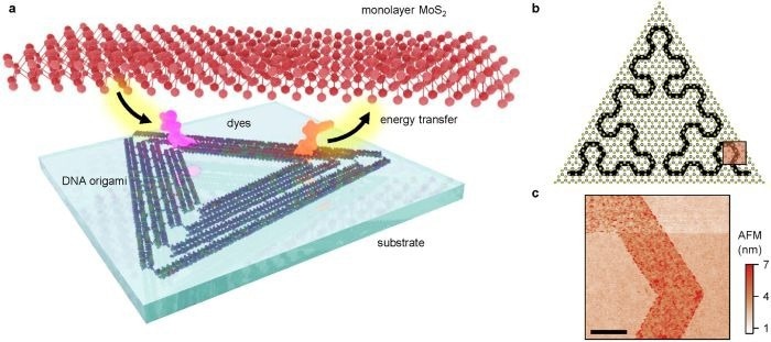
Skoltech researchers and their colleagues from Ludwig Maximilian University of Munich, Germany, Nanjing University of China, and the National Institute for Materials Science of Japan have developed a method for depositing organic molecules on a two-dimensional semiconductor in a highly controlled manner. Tested in this proof-of-concept study, the technique uses self-assembled DNA origami nanostructures to carry organic dye molecules in a predefined pattern covered by a 2D semiconductor. In the future, the technique could be used to create components for ultrasmall high-performance devices. The research paper came out in the journal Small Methods.
Originally inspired by graphene, a new class of atomically thin semiconductor materials – such as molybdenum disulfide – promises to enable electronic and optical devices that are smaller and more efficient than those achievable with conventional semiconductors like silicon. However, operating at such a small scale introduces a significant nanopatterning challenge: Creating well-defined, functional pathways within a two-dimensional material requires a level of precision that pushes the limits of current fabrication techniques.
“There are two basic approaches to creating a ‘landscape’ on a 2D semiconductor sheet to guide the conduction of excitons along preferred paths: Either you introduce some sort of defects that alter the initially uniform structure of the material, which is so far not possible to do with nanometer precision, or you deposit organic molecules on the monolayer, but until now it hasn’t been done in a controlled way, and the randomness of the resulting pattern puts a limitation on the device efficiency,” said study co-author Assistant Professor Irina Martynenko from Skoltech Physics.
The team successfully demonstrated a way of depositing organic dye molecules on a monolayer of molybdenum disulfide using the technique of DNA origami. It involves designing DNA nanostructures approximately 100 nanometers in size that carry dye molecules at predefined positions. The resulting construct is placed on a chip and covered by a 2D semiconductor.
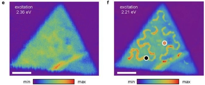
Image. Photoluminescence map of a triangular flake of atomically thin molybdenum disulfide with (right) and without (left) the underlying DNA origami-dye pattern’s contribution. The dye molecules carried by DNA clearly affect light emission across the flake. Credit: Shen Zhao et al./Small Methods
“Our experiments show that, firstly, the DNA origami-dye structures do assemble correctly and, second, the dye molecules and the molybdenum disulfide monolayer indeed exhibit the phenomenon of Förster resonance energy transfer. This is what enables the energy exchange between the two materials and therefore allows the semiconductor’s properties to be structured at the nanoscale by the deposited pattern. You can see this in photoluminescence images where a triangular molybdenum disulfide flake displays more or less uniform light emission at a wavelength not relevant for the dye molecules deposited behind the flake, but clearly emits more light in regions where the dye molecules absorb light,” said one of the study’s authors, Associate Professor Anvar Baimuratov from Skoltech Physics.
Now that the team has confirmed that DNA origami can be used to precisely and reliably pattern the energy landscape of two-dimensional semiconductors at the nanoscale, the researchers will attempt to create specific nanoelectronic and nanophotonic devices using this technique. Eventually, such nanostructured hybrid materials could enable the design of compact high-performance devices for optical computation and quantum simulations, light detection, etc.