Close Menu
  • News
    • Medical
    • Nanomaterials
    • AI & Robotics
    • 2D Materials
    • Metamaterials
    • Nanoelectronics
    • ETF’s
    • Medicine
  • Environment
    • Earth.com
    • TreeHugger
    • Nanomuscle
  • Beauty
    • Makeupanalysis
What's Hot

NY Creates Begins Installation of First Major Tool for High NA EUV Lithography Center at Albany Nanotech Complex

May 7, 2026

Orange Leaf Extract Produces Greener Antibacterial Nanoparticles

April 9, 2026

Pittcon’s First San Antonio Experience a Roaring Success

April 8, 2026
Facebook X (Twitter) Instagram
  • Contact Us
  • Privacy Policy
  • Terms & Conditions
Facebook X (Twitter) Instagram
Elnano – Global Innovative Nanotechnology SolutionsElnano – Global Innovative Nanotechnology Solutions
  • News
    • Medical
    • Nanomaterials
    • AI & Robotics
    • 2D Materials
    • Metamaterials
    • Nanoelectronics
    • ETF’s
    • Medicine
  • Environment
    • Earth.com
    • TreeHugger
    • Nanomuscle
  • Beauty
    • Makeupanalysis
Elnano – Global Innovative Nanotechnology SolutionsElnano – Global Innovative Nanotechnology Solutions
Home » New Microtronic WaferWeight Precisely Monitors Semiconductor Wafer Mass During Macro Defect Inspection
Nanoelectronics

New Microtronic WaferWeight Precisely Monitors Semiconductor Wafer Mass During Macro Defect Inspection

September 19, 2025No Comments2 Mins Read
Share
Facebook Twitter LinkedIn Pinterest Email

Microtronic, maker of advanced macro defect inspection systems and software, has announced a convenient and highly precise way to monitor the weights of semiconductor wafers at the same time as defects are being inspected – all on a single tool. This patented capability is called WaferWeight and it integrates fully into Microtronic’s EAGLEview™ line of high-speed macro defect inspection systems. It can be added to the latest EAGLEview 6 and also to previous models of the tool.

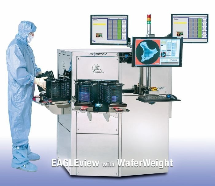
Image Credit: Microtronic

“Wafer mass metrology has become increasingly important as semiconductor processes have become more complex and sensitive,” said Microtronic CEO Reiner Fenske in making the announcement. “Today’s fabs would like to be able to measure the wafer mass changes that occur during processing, especially in deposition, etch, plating, backgrinding, bonding, TSV, and similar steps. However, previous wafer weight measurement methods have been slow and expensive, requiring a separate tool. Now, WaferWeight allows fabs to track wafer mass quickly, accurately, and economically – concurrently with macro defect inspection. Our EAGLEview can do defect inspection and wafer weighing both at the same time, on a single system.”

“And throughput speed plays an essential role in this process,” Fenske added. “In order to monitor changes in wafer weight, fabs really need to obtain data from every single wafer in every single lot. It is the exceptional speed of the EAGLEview that makes this possible. Which is why many top-tier fabs around the world have already chosen to incorporate our WaferWeight capability.”

The new WaferWeight measurements may have a resolution as low as 0.1mg. This allows precise tracking of changes in wafer mass between process steps – and also between different wafers in a lot. Monitoring wafer weight at various points throughout processing can be invaluable for discovering certain process problems that cannot be detected visually. A wafer weight change that exceeds allowable ranges can immediately flag an issue that needs further inspection or correction. Comprehensive wafer weight information can also be included in SPC systems to enhance the precision and quality of a fab’s process monitoring overall.

See also  Electrons Flow Like Liquid in Graphene: New Study Insights

WaferWeight information can all be stored in EAGLEview’s powerful ProcessGuard™ software. This system maintains a database of information on every wafer run through the tool – by lot, date and time. It can automatically randomize wafers and track incoming and outgoing slot positions of every wafer. ProcessGuard’s integrated Slot-Positional Analysis Tool can plot and compare a range of wafer information, including wafer weight. It can provide wafer weights and pre/post process weight deltas for every slot position.

Source link

Defect Inspection Macro Mass Microtronic Monitors Precisely semiconductor Wafer WaferWeight
Share. Facebook Twitter Pinterest LinkedIn Tumblr Email

Related Posts

6-Channel Piezo Driver for Precision Actuators & Transducers

April 6, 2026

Scientists Marry DNA Origami and 2D Materials to Make Nanoelectronics

April 3, 2026

PI Introduces Compact Alignment Engine for Wafer Testing

April 3, 2026

Establishing a Global Benchmark for Graphene Quality Control

April 2, 2026
Add A Comment

Comments are closed.

Top Posts

Study Shows a Plasmon-Induced Route to Advanced Hybrid Nanomaterials

October 14, 2025

‘Designing Defects’ in Graphene Opens New Possibilities for Future Tech

September 24, 2025

Sensor platform uses nanopore ‘speed cameras’ to pinpoint gases in complex mixtures

September 30, 2025

Subscribe to Updates

Get the latest sports news from SportsSite about soccer, football and tennis.

Explore the future with our Nanotech blog—covering innovations, research, applications, and breakthroughs shaping science, medicine, and modern technology.

We're social. Connect with us:

Facebook X (Twitter) Instagram YouTube
Top Insights

NY Creates Begins Installation of First Major Tool for High NA EUV Lithography Center at Albany Nanotech Complex

May 7, 2026

Orange Leaf Extract Produces Greener Antibacterial Nanoparticles

April 9, 2026

Pittcon’s First San Antonio Experience a Roaring Success

April 8, 2026

Subscribe to Updates

Get the latest creative news from FooBar about art, design and business.

  • Contact Us
  • Privacy Policy
  • Terms & Conditions

© 2026 elnano.com - All rights reserved.

Type above and press Enter to search. Press Esc to cancel.