


Silicon carbide (SiC) is composed of pure silicon (Si) and carbon (C). Its ability to adopt different crystalline polytypes results in a wide bandgap. Although SiC is a semiconductor with an indirect bandgap, it is used in several high-performance electronic and optical devices owing to its unique physical and electronic properties. This article discusses the characteristics of SiC, which makes it a promising material for nanotechnology applications.
Image Credit: luchschenF/Shutterstock.com
Importance of SiC
Individually, Si and C are essential elements for sustaining life. SiC, a compound of silicon and carbon, is a wide band gap IV-IV semiconductor with superior characteristics, including high-power, high-temperature, and high-frequency electronic applications.
SiC has over 200 crystalline forms, and the most common types are 3C, 6H, and 4H, which have bandgaps of 2.2, 3.02, and 3.20 eV, respectively. SiC can adopt different crystalline polytypes to monitor the band gap, which controls its electronic optical properties.
SiC has high chemical stability, enabling it to withstand harsh environments. SiC is the most biocompatible material and is used in blood-contacting and cardiovascular biomedical devices.
SiC exhibits outstanding thermal conductivity, low thermal expansion, and good thermal shock resistance. Additionally, the corrosion resistance, high hardness, and stiffness of SiC allow its wide range of industrial applications, especially in fields where corrosion resistance and wear are crucial requirements.
Properties of SiC
- Polytypism of SiC: SiC is known for its polytypism (different crystalline structures), generated by the stacking of Si and C along the principal axis (C-axis). The AaBbCcAaBbCc stacking generates a 3C-SiC zinc-blende lattice, AaBbAaBb generates 2H-SiC with a wurtzite lattice, and AaBbAaCcAaBbAaC generates a 4H-SiC lattice. Different crystalline forms with varying numbers of atoms per unit cell affect the physical properties of polytypes owing to the varying electronic energy bands and vibrational branches.
- Band Structure: Different crystalline forms of SiC have varying bandgap sizes, ranging from 2.4 eV (3C-SiC) to 3.35 eV (2H-SiC), which are crucial for determining their electronic and optical properties. SiC polytypes are indirect semiconductors, which means that the polytype with the smallest bandgap (3C-SiC ) to that with the largest bandgap (2H-SiC) requires the participation of phonons (quantized vibrational modes). Although SiC polytypes are indirect semiconductors, they are excellent candidates for power applications.
- Doping: Doping is a physical method used to obtain the desired electrical properties of SiC. In this process, an element, either an acceptor (aluminum/boron/gallium) or a donor (nitrogen/phosphorus), is introduced at the crystal growth stage to alter its conductivity. Since diffusion is not a feasible method to dope SiC, ion implantation with dopant activation via high-temperature heating is used to dope SiC. Previous studies reported the success of doping SiC with nitrogen for applications such as reducing power loss in vertical power device structures and high-frequency applications.
- Electrical Properties: Unintentional doping with nitrogen donors during the growth process indicates that they have excess electrons during the growth process, revealing n-type conductivity in SiC. Doped nitrogen atoms replace carbon atoms at lattice sites, varying the ionization energies owing to differing local environments and a specific interference effect. Furthermore, Hall measurements help determine the concentration of nitrogen donors, assuming an equal distribution among various lattice sites.
- Chemical Stability: SiC undergoes facile oxidation and forms a silicon dioxide (SiO2) film, which gradually hinders the oxidation process. However, if substances that can remove or break the silicon dioxide film exist simultaneously, SiC can be oxidized further. SiC does not easily dissolve in acids or bases but can be easily attacked by alkaline melts. The primary impurities found in SiC include C and SiO2 and the amount of impurities varies depending on the product type.
Methods of Growing Single Crystal SiC
Naturally, SiC is found in minute quantities in certain meteorites in the form of moissanites. Hence, most SiC available is synthesized synthetically. The traditional Acheson process for synthesizing SiC results in the formation of various crystalline forms and purities. Another conventional method of SiC synthesis is carbothermal reduction. However, this method requires a large amount of energy.
Alternative methods to prepare SiC single crystals include the following.
- Physical Vapor Transport (PVT): Also known as seeded sublimation growth, PVT is a successful method for growing large SiC single crystals. In this method, the SiC source material undergoes sublimation to transport Si and C atoms, which are reconstituted into a single crystal.
- Chemical Vapor Deposition (CVD): This is the most suitable method for depositing materials in the form of powders, thin films, or nanorods. Chemical reactions involved in the exchange of precursors for materials include thermolysis, hydrolysis, and oxidation.
- Sol–gel Process: This method for SiC synthesis results in the production of highly pure products with extremely uniform and dispersed microstructures that are difficult to achieve using conventional techniques. This method involves two steps: hydrolysis and polycondensation.
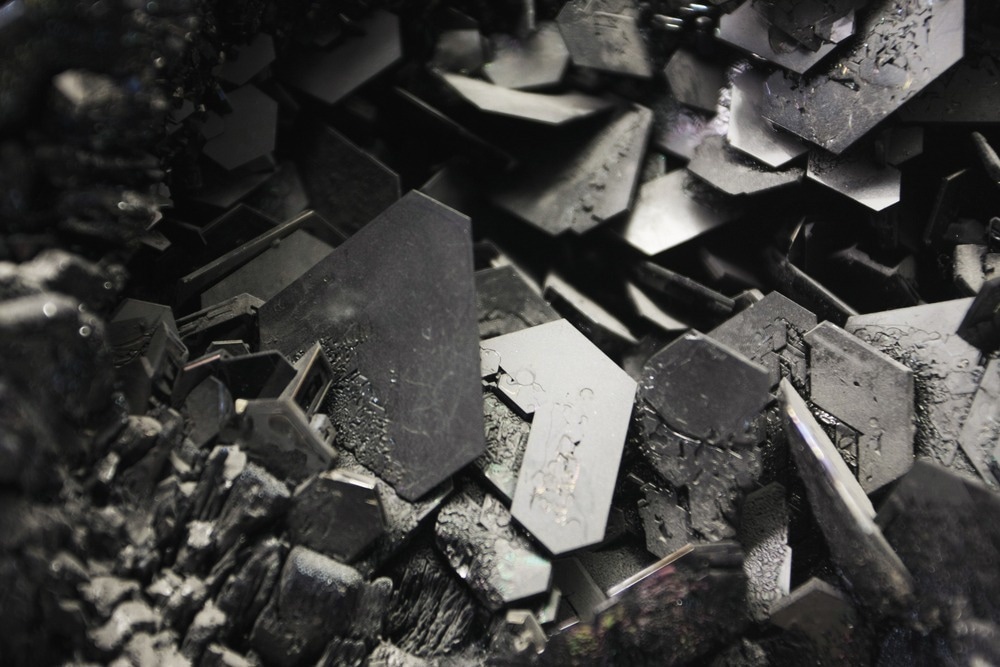
Image Credit: Zoltan Major/Shutterstock.com
Recent Trends in SiC Applications- Nanotechnology Relevance
SiC nanoparticles have high purity, thermal conductivity, stability, good wear resistance, and a small thermal expansion coefficient. Hence, the SiC nanoparticles are applied as follows:
- Manufacturing of rubber tires.
- Manufacturing grinding material with high hardness.
- It is also used as a high-grade refractory material.
- Manufacturing of high temperature-resistant sealing valves and nozzles
- Altering the strength of alloys.
- Mirror coatings in environments with high ultraviolet exposure.
An article published in Nanomaterials reported the direct amino-termination of aqueous SiC nanoparticles and demonstrated its applicability by attaching the synthesized nanoparticles to bovine serum albumin to exemplify functionalization. These nanoparticles showed intense fluorescence, indicating their potential application as fluorescent biomarkers.
Another article published in Nanotechnology Perceptions reported the fabrication of composite materials with high thermal conductivity and good mechanical strength, obtained by the electrosintering of aluminum oxide and SiC nanopowders.
Conclusion
Overall, SiC is a semiconducting material that exists in more than 250 different crystalline forms, called polytypes. The most common polytypes are 3C, 6H, and 4H. Its chemical, mechanical, and thermal properties are a good fit to make SiC a semiconductor of choice in harsh environments.
Furthermore, the high thermal conductivity, purity, stability, and outstanding wear resistance of SiC nanoparticles allowed their extensive application in electronics, ceramics, optics, and pharmaceuticals.
References and Further Reading
Sahu, T., et al. (2012). Diverse role of silicon carbide in the domain of nanomaterials. International Journal of Electrochemistry, 2012. Available at: https://www.hindawi.com/journals/ijelc/2012/271285/
Choyke, W. J., & Pensl, G. (1997). Physical properties of SiC. Mrs Bulletin, 22(3), pp. 25-29. doi.org/10.1557/S0883769400032723
Silicon Carbide Properties. (Accessed on 08 October 2023). Available at: https://www.washingtonmills.com/silicon-carbide/sic-properties
Silicon Carbide (SiC) Properties and Applications. (Accessed on 08 October 2023). Available at: https://www.azom.com/article.aspx?ArticleID=42
Silicon Carbide (SiC) Nanoparticles – Properties, Applications. (Accessed on 08 October 2023). Available at: https://www.azonano.com/article.aspx?ArticleID=3396
Czene, S., et al. (2023) Amino-Termination of Silicon Carbide Nanoparticles. Nanomaterials, 13, p.1953. doi.org/10.3390/nano13131953.
