by ARC Centre of Excellence in Future Low-Energy Electronics Technologies (FLEET)
A recent UNSW-led paper published in Nature Communications presents an exciting new way to listen to avalanches of atoms in crystals.
The nanoscale movement of atoms when materials deform leads to sound emission. This so-called crackling noise is a scale-invariant phenomenon found in various material systems as a response to external stimuli such as force or external fields.
Jerky material movements in the form of avalanches can span many orders of magnitude in size and follow universal scaling rules described by power laws. The concept was originally studied as Barkhausen noise in magnetic materials and now is used in diverse fields from earthquake research and building materials monitoring to fundamental research involving phase transitions and neural networks.
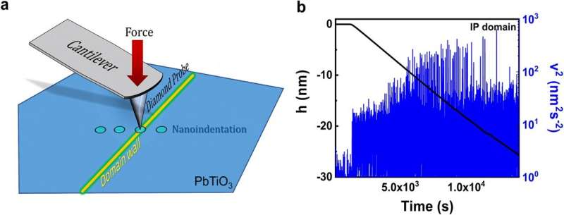
The new method for nanoscale crackling noise measurements developed by UNSW and University of Cambridge researchers is based on SPM nanoindentation.
“Our method allows us to study the crackling noise of individual nanoscale features in materials, such as domain walls in ferroelectrics,” says lead author Dr. Cam Phu Nguyen. “The types of atom avalanches differ around these structures when the material deforms.”
One of the method’s most intriguing aspects is the fact that individual nanoscale features can be identified by imaging the material surface before indenting it. This differentiation enables new studies that were not possible previously.
In a first application of the new technology the UNSW researchers have used the method to investigate discontinuities in ordered materials, called domain walls.
“Domain walls have been the focus of our research for some time. They are highly attractive as building blocks for post-Moore’s law electronics,” says author Prof Jan Seidel, also at UNSW. “We show that critical exponents for avalanches are altered at these nanoscale features, leading to a suppression of mixed-criticality, which is otherwise present in domains.”
From the perspective of applications and novel material functionalities, crackling noise microscopy presents a new opportunity for generating advanced knowledge about such features at the nanoscale. The study discusses experimental aspects of the method and provides a perspective on future research directions and applications.
Provided by
ARC Centre of Excellence in Future Low-Energy Electronics Technologies (FLEET)


