
Close Menu
  • News
    • Medical
    • Nanomaterials
    • AI & Robotics
    • 2D Materials
    • Metamaterials
    • Nanoelectronics
    • ETF’s
    • Medicine
  • Environment
    • Earth.com
    • TreeHugger
    • Nanomuscle
  • Beauty
    • Makeupanalysis
What's Hot

PI XYZ Nanopositioning Stage Delivers 1 Å Resolution – P-733

September 1, 2026

Researchers Identify the Best Nanographite Dose for SLA Resin

September 1, 2026

Nanoscale “Defects” Unlock a Major Heat Transfer Breakthrough

September 1, 2026
Facebook X (Twitter) Instagram
  • Contact Us
  • Privacy Policy
  • Terms & Conditions
Facebook X (Twitter) Instagram
Elnano – Global Innovative Nanotechnology SolutionsElnano – Global Innovative Nanotechnology Solutions
  • News
    • Medical
    • Nanomaterials
    • AI & Robotics
    • 2D Materials
    • Metamaterials
    • Nanoelectronics
    • ETF’s
    • Medicine
  • Environment
    • Earth.com
    • TreeHugger
    • Nanomuscle
  • Beauty
    • Makeupanalysis
Elnano – Global Innovative Nanotechnology SolutionsElnano – Global Innovative Nanotechnology Solutions
Home » PI XYZ Nanopositioning Stage Delivers 1 Å Resolution – P-733
Nanomaterials

PI XYZ Nanopositioning Stage Delivers 1 Å Resolution – P-733

September 1, 2026No Comments3 Mins Read
Share
Facebook Twitter LinkedIn Pinterest Email

High-precision XYZ piezo stage designed for super-resolution microscopy, AFM, surface metrology, and advanced imaging.
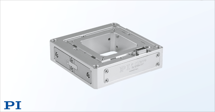
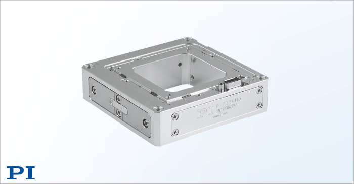
PI’s P-733 XYZ nanopositioning stage delivers 1 Å resolution for super-resolution microscopy, AFM, surface metrology, and advanced imaging applications. Image Credit: PI (Physik Instrumente) LP

PI (Physik Instrumente), a global leader in precision motion control and nanopositioning technology, offers the P-733 XYZ piezo nanopositioning stage, delivering 0.1 nm (1 Å) positioning resolution for demanding applications in super-resolution microscopy, atomic force microscopy (AFM), surface nanometrology, and advanced imaging.

The P-733 combines frictionless flexure guidance with high-accuracy capacitive position feedback to achieve sub-nanometer positioning performance and highly repeatable motion. Travel ranges of up to 100 × 100 µm in X and Y and 10 µm in Z enable precision sample scanning and measurement across comparatively large areas. A 50 × 50 mm clear aperture supports transmitted-light microscopy and other optical imaging techniques.

High-Stiffness Direct-Drive Version for Maximum Throughput

For applications that demand the highest scanning speeds and fastest settling times, the P-733.3DD direct-drive version provides 30 × 30 × 10 µm travel with the same 0.1 nm resolution. Its high-stiffness design supports rapid scanning and dynamic positioning, with resonant frequencies exceeding 1 kHz.

The stage architecture incorporates parallel kinematics and parallel metrology, ensuring that all motion axes are measured relative to a common fixed reference. This design actively compensates for crosstalk and guiding errors, helping maintain nanometer-level tracking accuracy during high-speed scanning and precision measurement tasks.

Key Features

  • 0.1 nm (1 Å) positioning resolution
  • UHV-compatible and nonmagnetic versions available
  • XYZ motion with travel ranges up to 100 × 100 × 10 µm
  • 50 × 50 mm clear aperture for transmitted-light microscopy
  • Capacitive feedback sensors with up to 99.97% motion linearity
  • Parallel kinematics and parallel metrology for enhanced multi-axis accuracy
  • High-stiffness direct-drive variant for fast scanning and shortest step-and-settle times
  • Ideal for wafer metrology, super-resolution microscopy, nanoimprinting, surface metrology, and image stabilization
See also  Twisted Graphene Shows Unconventional Superconductivity

Wear-Free Design for Long-Term Stability

The P-733 employs wear-free, zero-play flexure guides and PICMA® multilayer piezo actuators, eliminating mechanical friction and backlash. Noncontact capacitive sensors provide highly linear position measurement with exceptional long-term stability and typical linearity of 99.97%.

Applications and Industries Served

The P-733 is designed for a broad range of industrial and scientific applications, including super-resolution and confocal microscopy, AFM, surface characterization, wafer positioning, nanoimprinting, micromanipulation, precision optics, and image stabilization. Ultra-high-vacuum-compatible and nonmagnetic configurations are available for specialized environments. Markets and Applications. In addition to super-resolution and confocal microscopy, the P-733 is suitable for surface measurement, wafer positioning, nanoimprinting, micromanipulation, and image stabilization. Ultra-high-vacuum-compatible and nonmagnetic versions are available on request.

Source:

PI (Physik Instrumente) LP

Source link

delivers Nanopositioning P733 resolution Stage XYZ
Share. Facebook Twitter Pinterest LinkedIn Tumblr Email

Related Posts

Biomass-Derived Nanomaterials Offer a Greener Route to Pollution Cleanup

September 1, 2026

PI Accepts Gold in MassEcon Economic Impact Awards at Gillette Stadium in Foxborough, MA

August 31, 2026

NY Creates Begins Installation of First Major Tool for High NA EUV Lithography Center at Albany Nanotech Complex

May 7, 2026

Ultrafast Electron Microscopy Captures the Intricate Dynamics of Plasmonic Nanostructures

April 7, 2026
Add A Comment
Leave A Reply Cancel Reply

Top Posts

Efficient PVP Replacement for Silver Nanowires Developed

November 11, 2025

Targeting Nanoparticles for Heart Repair

September 19, 2025

PI’s Precision Motion Control: Essentials with Fast Delivery

September 19, 2025

Subscribe to Updates

Get the latest sports news from SportsSite about soccer, football and tennis.

Explore the future with our Nanotech blog—covering innovations, research, applications, and breakthroughs shaping science, medicine, and modern technology.

We're social. Connect with us:

Facebook X (Twitter) Instagram YouTube
Top Insights

PI XYZ Nanopositioning Stage Delivers 1 Å Resolution – P-733

September 1, 2026

Researchers Identify the Best Nanographite Dose for SLA Resin

September 1, 2026

Nanoscale “Defects” Unlock a Major Heat Transfer Breakthrough

September 1, 2026

Subscribe to Updates

Get the latest creative news from FooBar about art, design and business.

  • Contact Us
  • Privacy Policy
  • Terms & Conditions

© 2026 elnano.com - All rights reserved.

Type above and press Enter to search. Press Esc to cancel.