Close Menu
  • News
    • Medical
    • Nanomaterials
    • AI & Robotics
    • 2D Materials
    • Metamaterials
    • Nanoelectronics
    • ETF’s
    • Medicine
  • Environment
    • Earth.com
    • TreeHugger
    • Nanomuscle
  • Beauty
    • Makeupanalysis
What's Hot

NY Creates Begins Installation of First Major Tool for High NA EUV Lithography Center at Albany Nanotech Complex

May 7, 2026

Orange Leaf Extract Produces Greener Antibacterial Nanoparticles

April 9, 2026

Pittcon’s First San Antonio Experience a Roaring Success

April 8, 2026
Facebook X (Twitter) Instagram
  • Contact Us
  • Privacy Policy
  • Terms & Conditions
Facebook X (Twitter) Instagram
Elnano – Global Innovative Nanotechnology SolutionsElnano – Global Innovative Nanotechnology Solutions
  • News
    • Medical
    • Nanomaterials
    • AI & Robotics
    • 2D Materials
    • Metamaterials
    • Nanoelectronics
    • ETF’s
    • Medicine
  • Environment
    • Earth.com
    • TreeHugger
    • Nanomuscle
  • Beauty
    • Makeupanalysis
Elnano – Global Innovative Nanotechnology SolutionsElnano – Global Innovative Nanotechnology Solutions
Home » Cost-Optimized, High-Speed Fiber-Alignment System for Silicon Photonics
Nanoelectronics

Cost-Optimized, High-Speed Fiber-Alignment System for Silicon Photonics

November 12, 2025No Comments2 Mins Read
Share
Facebook Twitter LinkedIn Pinterest Email

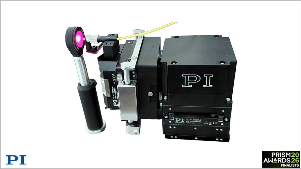
PI (Physik Instrumente) offers a new 6-axis variant of its successful F-141 PINovAlign automated fiber alignment system. The F-141 is a compact, cost-optimized high-performance alignment solution providing precision motion in 2, 3, 4 and degrees of freedom for the industrial test and assembly of photonic integrated circuits (PICs), fibers and fiber array units (FAU). Designed for space-limited environments, the F-141 fits within a footprint of just 5 x 7 x 4 inches (WxLxH) while delivering 40 mm of XYZ travel and ±12° of rotation – ideal for array alignment tasks.

The F-141 PINovAlign is a cost-optimized, high-speed photonics alignment system available in 3 to 6-axis single- and dual-sided variants. The PINovAlign system is ideal for array alignment and silicon photonics applications. Image Credit: PI (Physik Instrumente) LP

Direct-Drive Design Provides for High Dynamics

Powered by direct-drive motors, the system achieves high acceleration, speed, and resolution with long lifetime and maintenance-free operation. Crossed-roller bearings and flexure guides ensure smooth, precise motion and repeatable performance.

Optional 6-Axis Version

In addition to 2-, 3-, and 4-axis models, the F-141 is available with an optional pitch/yaw module for fully automated six-degree-of-freedom alignment. Custom configurations are also available for different optical axis orientations.

Advanced Alignment Control and Integrated Intelligence

The F-141 is driven by PI’s EtherCAT®-based multi-axis alignment controller, featuring rapid signal analysis and onboard machine learning. Embedded scan and alignment routines deliver faster and more reliable results than conventional host-based algorithms, simplifying system integration and boosting throughput.

Fastest First-Light Detection in the Industry

PI’s proprietary alignment algorithms enable industry-leading first-light acquisition and signal optimization speeds – up to 100× faster than conventional techniques. Leveraging ultra-low-noise electronics, pulse-width modulation (PWM) amplifiers, and 24-bit analog-to-digital converters for high-bandwidth optical power monitoring, the F-141 delivers highly stable and repeatable optical coupling performance, even under challenging environmental conditions.

See also  Electrified atomic vapor system enables new nanomaterial mixtures

SPIE Prism Award Finalist

The F-141 PINovAlign system was also recognized as a finalist for the SPIE Prism Award in the Test & Measurement category. The winners will be announced in January 2026, during the Photonics West Conference in San Francisco.

Industries Served

PIC alignment, fiber alignment, photonics test and assembly, optical component assembly, automated photonic wafer testing, photonics wafer probing

Source:

PI (Physik Instrumente) LP

Source link

CostOptimized FiberAlignment HighSpeed Photonics silicon System
Share. Facebook Twitter Pinterest LinkedIn Tumblr Email

Related Posts

Possible Dual-Channel Encryption with Silicon Metasurfaces

April 6, 2026

6-Channel Piezo Driver for Precision Actuators & Transducers

April 6, 2026

Scientists Marry DNA Origami and 2D Materials to Make Nanoelectronics

April 3, 2026

PI Introduces Compact Alignment Engine for Wafer Testing

April 3, 2026
Add A Comment

Comments are closed.

Top Posts

Scientists develop hydrogel platform for long-lasting, precision drug delivery

September 18, 2025

What really happens during catalysis

September 18, 2025

30 TB hard drive launched by Seagate

September 19, 2025

Subscribe to Updates

Get the latest sports news from SportsSite about soccer, football and tennis.

Explore the future with our Nanotech blog—covering innovations, research, applications, and breakthroughs shaping science, medicine, and modern technology.

We're social. Connect with us:

Facebook X (Twitter) Instagram YouTube
Top Insights

NY Creates Begins Installation of First Major Tool for High NA EUV Lithography Center at Albany Nanotech Complex

May 7, 2026

Orange Leaf Extract Produces Greener Antibacterial Nanoparticles

April 9, 2026

Pittcon’s First San Antonio Experience a Roaring Success

April 8, 2026

Subscribe to Updates

Get the latest creative news from FooBar about art, design and business.

  • Contact Us
  • Privacy Policy
  • Terms & Conditions

© 2026 elnano.com - All rights reserved.

Type above and press Enter to search. Press Esc to cancel.