Multiphoton lithography (MPL) is a technique that uses ultra-short laser pulses to create complex three-dimensional (3D) structures at the micro- and nanoscale. It is based on the principle of multiphoton absorption (MPA), which occurs when two or more photons are simultaneously absorbed by a molecule, resulting in a nonlinear optical process.
By focusing the laser beam on a photosensitive material, such as a photoresist or a prepolymer, the multiphoton absorption induces a localized chemical reaction that changes the properties of the material. By scanning the laser beam and/or translating the sample in three dimensions, the desired shape can be fabricated with high resolution and accuracy without any geometrical restrictions. This enables the realization of laser 3D nanoprinting as an additive manufacturing technique.
MPL has already many applications in fields such as micro-optics, nanophotonic devices, metamaterials, integrated chips and tissue engineering. It can create structures that are impossible or difficult to achieve by conventional lithography methods, such as curved surfaces, hollow structures, and functional gradients. It can also enable the fabrication of novel materials with tailored optical, mechanical and biological properties.
Despite the MPL setups are commercially available, the understanding of photophysical and photochemical mechanisms is still controversial, as most common laser sources are chosen to be of 800 nm wavelength while others popular ones of 515 nm or 1,064 nm were also shown to be suitable.
However, the single and most popular theory of two-photon absorption cannot be applied to explain all the different experimental conditions and the produced outcome. This issue is important for the further development of the laser sources and the construction of high-throughput 3D nanoprinting machines oriented for industrial demands.
Experiment and findings
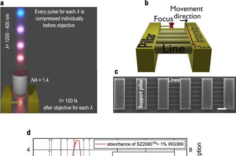
We studied MPL, also widely known as two-photon polymerization (2PP) or simply laser 3D nanoprinting, using a wavelength-tunable femtosecond laser. We found that we could use any color of the spectrum from 500 to 1,200 nm with a fixed pulse width of 100 fs to achieve an interplay of photophysical mechanisms more delicate than just two-photon photopolymerization.
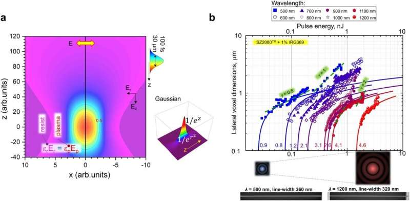
We assessed the effective order of absorption, i.e., the X-photon absorption, as well as optimal exposure conditions for photosensitized and pure SZ2080 pre-polymer. We discovered that the tunability of wavelength greatly influenced the dynamic fabrication window (DFW), resulting in a 10-fold increase when optimized.
Moreover, we observed a non-trivial energy deposition by X-photon absorption with an onset of a strong lateral size increase at longer wavelengths and explained that it was due to reaching epsilon-near-zero (ENZ) conditions. Such a control over the voxel aspect ratio and, consequently, the photopolymerized volume, may boost 3D nanoprinting efficiency.

We also investigated the evolution of the polymerized volume during direct laser writing (DLW) via different energy delivery mechanisms: one-/two-/three-photon absorption, avalanche ionization and thermal diffusion leading to controlled photo-polymerization. We showed that 3D nanolithography with ultra-short pulses at a wide visible-to-near-IR spectral range of 400–1,200 nm proceeds via multiphoton excitation defined by effective order of absorption. Our research is published in the journal Virtual and Physical Prototyping.
Revelation
We noted that the lateral voxel size deviated from the analytical curve and had a distinct step-like onset most expressed at longer wavelengths and higher power. We attributed this to ENZ state formation at the focal region that caused a larger portion of incident light intensity to be absorbed yielding a large lateral cross-section of photopolymerized single voxel (deduced form line feature).
We have validated our approach in an SZ2080 as a model material and suggested that it should be viable with other widespread materials such as commercial IP photoresins, PETA and other cross-linkable materials. We demonstrated the applications of this technique in various fields such as micro-optics, nanophotonic devices, metamaterials, integrated chips and tissue engineering.
We presented some examples of controlled refractive index, high transparency and resilient as well as active micro-optical components that are enabled by X-photon lithography in combination with calcination and atomic layer deposition. These achievements have immediate applications in sensing under harsh conditions, open space, and including unmanned aerial vehicles (UAV).
Impact
In perspective, we still need deeper investigations into the mechanism of heat accumulation, which is dependent on scan speed and laser repetition rate, as well as focal spot size. The tunable wavelength, together with pulse chirp, duration and burst-mode operation, which is becoming a standard in commercial fs-laser sources, can provide further improvements.
Considering the trend of the last 20 years of Moore’s law scaling with an average fs-laser power doubling every two years, the high-throughput applications will benefit from parameter-optimized 3D nano-printing.
This story is part of Science X Dialog, where researchers can report findings from their published research articles. Visit this page for information about ScienceX Dialog and how to participate.


