Discover the significance of stress measurement in thin films for industries like semiconductors and medical equipment, and explore various methods for precise quantification.
Image Credit: MelnikovSergei/Shutterstock.com
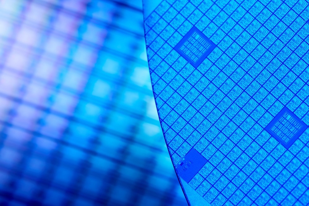
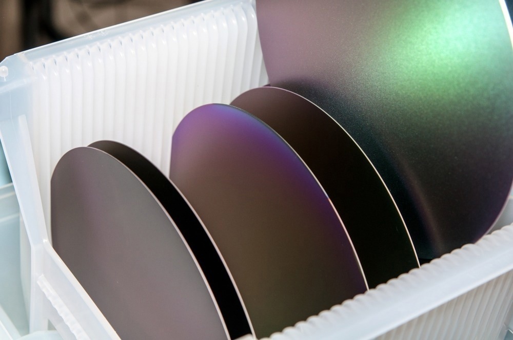
Thin films form the basis of many industries today, including semiconductors, electric vehicles, smart optical coatings, sophisticated medical equipment, and protective layers on high-temperature alloys. The functioning and reliability of thin film-based products are highly governed by stresses in the films, which may arise during and post-deposition processes. Hence, accurate methods are required for stress measurement in thin films for their practical applications.
Introduction to Stress Measurement in Thin Film Research
Materials in low-dimensional structures like thin films exhibit different properties than those in the bulk due to strain effects.1 Stress in thin films can be calculated using Hooke’s law, which defines it as proportional to strain.4 The stress in thin films on thick substrates can range from MPa to GPa, which is quite large compared to that found in their bulk counterpart.2
Before measurement, it is imperative to understand the numerous factors resulting in the stresses. Since films are generally deposited at elevated temperatures, substantial stress can develop while post-deposition cooling the film to room temperature due to the difference in thermal expansion between the film and substrate. Intrinsic stress can result even during the deposition process, which occurs under highly nonequilibrium conditions because the film temperature is often far below the material melting temperature.2
The nature of the stress highly depends on the deposition technique. For instance, sputtering yields compressed films, while films from chemical vapor deposition are tensed.2 Phase transformations, such as from amorphous to polycrystalline during post-deposition thermal treatments, may add to the film stress.2 The deformations that occur to thin films can be macroscopically measured in terms of a change in curvature on their surfaces.1
Significance of Stress Measurement in Thin Film Studies
Stress in thin films can lead to several problems, the most obvious being mechanical failure, i.e., cracking under tensile stress when the film is brittle. Stress can cause the failure of an interface between films in multilayer structures. A fracture can also be induced in the substrate itself due to stress in the film over it. 2
Stress in metal interconnection lines can lead to void formations, resulting in electrical failure. The band structure of a semiconducting substrate can be altered due to film stress, resulting in a modified electrical behavior of the device. Deformation of optical thin films in medical equipment can prove to be lethal. In the case of protective thin film oxides over high-temperature alloys, the film stressed beyond a critical value may delaminate and cease to protect the underlying metal. Therefore, precise measurement and control of stress during the fabrication process is essential in thin films. 2
Methods and Techniques for Stress Measurement in Thin Films
With recent technological advancements, several methods and techniques have evolved for near-to-exact stress measurements. These involve either measuring the substrate deformation produced by the stress in the film and then calculating the stress or measuring the strain in the film and then calculating the stress using Hooke’s law. The former method requires a knowledge of the film thickness, substrate thickness, and the elastic properties of the substrate, while the latter requires a knowledge of the elastic properties of the film itself. 2
The substrate deformation can be determined by measuring its profile, with and without the film of interest. This can be done mechanically using a profilometer, which is a highly sensitive method but has the obvious disadvantage of possibly damaging the film due to the probe being in direct contact with the sample surface. Additionally, the method is applicable only at ambient temperature. 2
Interferometry provides an alternative method by permitting a reasonable amount of free space above the sample surface so that measurements as a function of temperature are possible. It also eliminates the need for scanning, and the entire sample surface can be measured simultaneously. The sensitivity, however, is less than that attainable by other methods. 2
In the case of reflecting surfaces, a widely used technique involves measuring the deflection of a laser beam reflected from the sample as it is scanned across its surface. Multi-beam optical sensor (MOS) is one such stress measuring tool developed by k-Space ASSOCIATES, INC (USA) that uses a laser beam to measure the thin films’ curvature in situ optically during the deposition process. 1

Image Credit: fotografos/Shutterstock.com
Raman spectroscopy is also widely used to measure strain in silicon substrates with high spatial resolution. The sample is illuminated with a sharply focused laser beam, and the scattered light is measured with a Raman spectrometer. The characteristic frequencies of vibration change with interatomic distance; consequently, any elastic strain in the material changes the vibrational energy levels and produces corresponding shifts in the Raman spectrum. 2
In many cases, it is preferable to measure strain in the film directly as it eliminates the need to determine the film thickness, especially in cases where multiple films are present or the geometry is complex, e.g., patterned structures. Unfortunately, such measurements are usually more difficult and time-consuming, and the choice of experimental techniques is much more limited.
The most widely used direct method for crystalline films is determining the change in interplanar spacing by X-ray diffraction. Additionally, fluorescence spectroscopy (for example, fluorescence of chromium ions in alumina) has also been used for direct stress measurements in thin films. 2
Applications of Stress Measurement in Thin Film Characterization
Microstructural characteristics of thin films, such as grain size and grain morphology, thermal and electrical transport, and optical properties, can vary widely with deposition techniques. Internal residual stresses retained in thin films due to the deposition process significantly influence the microstructural properties of the films. As discussed above, these stresses can also result in buckling, cracking, or delamination, causing film failure. Hence, while studying the properties of a film, the material microstructure and its residual stress must be quantified simultaneously. Comprehending the relation of the deposited microstructure with its residual stress is essential to obtaining the desired thin film characteristics. 3
Crystalline defects, imperfect epitaxial layers, and a distorted film surface with features like hillocks and whiskers are possible outcomes of residual stresses, which, in turn, can alter film properties, including electrical conductivity, optical reflectivity and magnetization. It is impossible to avoid residual stress in thin films completely. Small amounts of residual stress may be tolerable in some applications as they may not significantly affect the operation and reliability of the device. Nonetheless, it is necessary to measure the amount of residual stress in thin films to optimize deposition parameters and ensure smooth device operation. 4
Therefore, stress measurement in thin films can give valuable insights into the forces in play and enhance our understanding of the related physics, possibly leading to other novel applications.
Methods for Measuring Thin Film Thickness
References and Further Reading
- Lababidi, A., & Wolff, M. (n.d.) Measuring Stress in Thin Films by a Multi-beam Optical Sensor (MOS), [Online] Uppsala University. Available at: https://uu.diva-portal.org/smash/get/diva2:1542460/FULLTEXT01.pdf
- Flinn, P. A. (2001). Thin Films: Stress Measurement Techniques. In NASA ADS. https://ui.adsabs.harvard.edu/abs/2001emst.book.9274F/abstract. doi.org/10.1016/b0-08-043152-6/01671-5
- Koenig, T.R., et al. (2021). The microstructural and stress evolution in sputter deposited Ni thin films. Surface and Coatings Technology, p. 412. doi.org/10.1016/j.surfcoat.2021.126973
- Waters, P. (2008). Stress Analysis and Mechanical Characterization of Thin Films for Microelectronics and MEMS Applications. [Online] USF Tampa Graduate Theses and Dissertations. Available at: https://digitalcommons.usf.edu/etd/558


