


Electron-beam lithography (e-beam lithography) is a high-precision nanofabrication technique used to produce patterns with features as small as a few nanometers. By using a focused beam of electrons to write directly onto a substrate coated with an electron-sensitive resist, e-beam lithography eliminates the need for templates, making it a highly adaptable tool for intricate designs.1
Image Credit: IM Imagery/Shutterstock.com
This method is widely applied in manufacturing nanostructures and devices on both conventional and irregular surfaces. Substrates like atomic force microscopy (AFM) tips, optical fibers, and porous Si3N4 membranes are commonly patterned using this technique, supporting advancements in chemical sensing, plasmonics, and quantum research.2
Its precision and versatility make e-beam lithography essential in nanotechnology, materials science, electronics, and biophotonics.
Principle of Operation
E-beam lithography operates on principles similar to photolithography but provides significantly higher resolution. The process begins with coating a substrate with an electron-sensitive resist material. A highly focused electron beam is then directed onto the resist-coated surface.
The electron beam is generated, accelerated to the desired working voltage, and carefully managed by electron-optical components housed within a vacuum-sealed column. These components are responsible for focusing the beam, switching it on and off, and deflecting it to accurately follow the specified pattern.3
As the beam scans the resist-coated surface, it transfers energy to the resist, triggering chemical changes in the exposed areas. The solubility of these regions depends on the type of resist used. For positive resists, exposure makes the areas more soluble in the developer solution. Conversely, for negative resists, exposure causes cross-linking, rendering the areas less soluble.3
This precise modulation of the beam allows for nanoscale patterning, creating extremely fine features essential for advanced nanofabrication. The entire process is controlled via computer-aided design (CAD) software, ensuring accuracy and precision in writing intricate patterns on the substrate.3
The Process
The e-beam lithography process involves several key steps: substrate preparation, pattern writing, development, and etching. Each step contributes to the successful transfer of high-resolution designs onto a substrate.
Substrate Preparation
The process begins with preparing the substrate, which is typically made of materials such as silicon, glass, or other semiconductor wafers. An electron-sensitive resist material, such as polymethyl methacrylate (PMMA), is then applied to the substrate. This is typically done through spin coating, a technique in which the substrate is spun at high speeds to form a thin, uniform resist layer.
After coating, the substrate undergoes a soft bake at temperatures between 130 °C and 170 °C to remove residual solvents and strengthen the adhesion of the resist to the substrate. This step is essential for ensuring precise patterning during subsequent stages.4-5
Pattern Writing
With the substrate prepared, the electron beam is used to write the desired pattern onto the resist. A highly focused electron beam scans the surface with exceptional precision, and its intensity and position are modulated by advanced computer software.
There are two primary approaches to pattern writing:
- Direct Writing: The electron beam writes the pattern directly onto the resist, scanning pixel by pixel. This method is highly flexible and can produce extremely fine features as small as 10 nanometers.
- Projection Printing: Systems such as Scattering with Angular Limitation in Projection Electron-Beam Lithography (SCALPEL) and Projection Reduction Exposure with Variable Axis Immersion Lenses (PREVAIL) use a mask to project a pattern onto the resist, allowing larger areas to be patterned simultaneously.3,5
Development
Following exposure, the substrate undergoes development to reveal the patterned features. The substrate is immersed in a developer solution that selectively dissolves specific areas of the resist.
- Positive Resists: The exposed areas become soluble and are removed during development.
- Negative Resists: The exposed areas undergo cross-linking and remain intact, while the unexposed regions are dissolved.
For example, a common developer for PMMA is a mixture of methyl isobutyl ketone (MIBK) and isopropanol (IPA). This step removes unwanted resist, leaving a relief structure that mirrors the design created by the electron beam. Careful control of the development process is essential to ensure high fidelity and accuracy in the final pattern.5-6
Etching
The final step in the e-beam lithography process is etching, where the developed resist pattern is transferred onto the substrate. Two main etching techniques are employed:
- Dry Etching: Methods such as plasma etching or reactive ion etching (RIE) use ionized gases to selectively remove material from the exposed regions of the substrate.
- Wet Etching: Chemical solutions are used to dissolve material in the exposed areas of the substrate.5-6
Once etching is complete, the remaining resist is removed using appropriate solvents, leaving the final patterned structure on the substrate. This structure is now ready for various applications, including microelectronics, photonics, and other nanotechnology fields.5,6
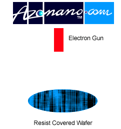
Figure 1. Basic illustration of how Electron Beam Lithography (EBL) works
Types of Electron-Beam Lithography
Serial Writing
Traditional e-beam lithography uses a serial writing process where a finely focused electron beam writes the pattern pixel by pixel onto a resist-coated substrate. This method can use a Gaussian beam, which scans the surface in a raster or vector fashion, or a shaped beam to create more complex patterns.3,7
Serial writing provides exceptional flexibility and resolution, enabling feature sizes below 10 nanometers. However, the process is inherently slow, especially for large or complex designs, as each pixel must be written individually.7 This low throughput makes serial writing less suitable for high-volume manufacturing in the semiconductor industry.
Parallel Writing
To address the limitations of serial writing, parallel writing techniques have been developed. These systems utilize multiple electron beams operating simultaneously, significantly increasing the speed of patterning while maintaining high resolution.
Technologies such as Multiple E-Beam Direct-Write (MEBDW) and Massively Parallel Electron Beam Direct-Write (MPEBDW) systems can utilize tens of thousands or even hundreds of thousands of electron beams.8 For example, systems like MAPPER lithography use over 650,000 beamlets and achieve throughputs of up to 40 wafers per hour.
Challenges such as beam alignment and uniformity persist; however, parallel writing demonstrates considerable potential to address the requirements of commercial semiconductor manufacturing and large-scale nanofabrication. These advancements enhance the practicality of e-beam lithography for industrial-scale applications.3, 9
Conclusion
Ongoing advancements in e-beam lithography are enhancing its efficiency and commercial applicability, solidifying its importance in advanced nanofabrication. Innovations such as parallel writing techniques are improving both speed and throughput, addressing the limitations of earlier methods.
The integration of emerging technologies and refinement of existing systems is expected to further expand its capabilities.3 These advancements establish e-beam lithography as an essential technology for driving progress in microelectronics, photonics, materials science, and healthcare, reinforcing its role in shaping 21st-century manufacturing.
A brief introduction to e-beam lithography
References and Further Readings
1. Zhu, C.; Ekinci, H.; Pan, A.; Cui, B.; Zhu, X. (2024). Electron Beam Lithography on Nonplanar and Irregular Surfaces. Microsystems & Nanoengineering. https://www.nature.com/articles/s41378-024-00682-9
2. Cui, Z. (2024). Electron Beam Lithography. Nanofabrication: Principles, Capabilities and Limits. https://link.springer.com/book/10.1007/978-0-387-75577-9
3. Sharma, E.; Rathi, R.; Misharwal, J.; Sinhmar, B.; Kumari, S.; Dalal, J.; Kumar, A. (2022). Evolution in Lithography Techniques: Microlithography to Nanolithography. Nanomaterials. https://www.mdpi.com/2079-4991/12/16/2754
4. Gangnaik, AS.; Georgiev, YM.; Holmes, JD. (2017). New Generation Electron Beam Resists: A Review. Chemistry of Materials. https://pubs.acs.org/doi/10.1021/acs.chemmater.6b03483
5. Tseng, AA.; Chen, K.; Chen, CD.; Ma, KJ. (2003). Electron Beam Lithography in Nanoscale Fabrication: Recent Development. IEEE Transactions on electronics packaging manufacturing. https://ieeexplore.ieee.org/document/1236879
6. Saifullah, MS.; Tiwale, N.; Ganesan, R. (2022). Review of Metal-Containing Resists in Electron Beam Lithography: Perspectives for Extreme Ultraviolet Patterning. Journal of Micro/Nanopatterning, Materials, and Metrology. https://www.spiedigitallibrary.org/journals/journal-of-micro-nanopatterning-materials-and-metrology/volume-21/issue-04/041402/Review-of-metal-containing-resists-in-electron-beam-lithography/10.1117/1.JMM.21.4.041402.full
7. Sebastian, EM.; Jain, SK.; Purohit, R.; Dhakad, S.; Rana, R. (2022). Nanolithography and Its Current Advancements. Materials Today: Proceedings. https://www.sciencedirect.com/science/article/abs/pii/S2214785320312608?via%3Dihub
8. Esashi, M.; Miyaguchi, H.; Kojima, A.; Ikegami, N.; Koshida, N.; Ohyi, H. (2022). Development of a Massively Parallel Electron Beam Write (Mpebw) System: Aiming for the Digital Fabrication of Integrated Circuits. Japanese Journal of Applied Physics. https://iopscience.iop.org/article/10.35848/1347-4065/ac4ce1/meta
9. de Boer, G.; Dansberg, M.; Jager, R.; Peijster, J.; Slot, E.; Steenbrink, S.; Wieland, M. (2013). Mapper: Progress toward a High-Volume Manufacturing System, Alternative Lithographic Technologies V. https://www.spiedigitallibrary.org/conference-proceedings-of-spie/8680/1/MAPPER-progress-toward-a-high-volume-manufacturing-system/10.1117/12.2011486.short
