Close Menu
  • News
  • Medical
  • Technology
  • Nanomaterials
  • Research
  • Blog
    • Nasiol.com
  • Contact
    • Tech7685@gmail.com
What's Hot

2D hybrid material integrates graphene and silica glass for next-generation electronics

June 4, 2025

Zeolite nanopore model links crystal size to metal cluster migration and catalyst performance

June 4, 2025

Spontaneous symmetry breaking in electron systems proves elusive

June 3, 2025
Facebook X (Twitter) Instagram
Nanotech – Nanomaterials | Medical | Research | News Stories Updated Daily Nanotech – Nanomaterials | Medical | Research | News Stories Updated Daily
  • News
  • Medical
  • Technology
  • Nanomaterials
  • Research
  • Blog
    • Nasiol.com
  • Contact
    • Tech7685@gmail.com
Facebook X (Twitter) Instagram
Nanotech – Nanomaterials | Medical | Research | News Stories Updated Daily Nanotech – Nanomaterials | Medical | Research | News Stories Updated Daily
Home»News»Visualizing the embedded twisted interfaces of two-dimensional materials
News

Visualizing the embedded twisted interfaces of two-dimensional materials

September 4, 2023No Comments3 Mins Read
Facebook Twitter Pinterest Telegram LinkedIn Tumblr WhatsApp Email
Visualizing the embedded twisted interfaces of two-dimensional materials
Share
Facebook Twitter LinkedIn Pinterest Telegram Email
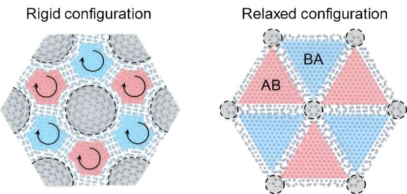
Schematics of the atomic structures before and after reconstruction of the twisted bilayer graphene. Credit: Science China Press

Vertically stacking two-dimensional (2D) materials to form van der Waals homo- or hetero-structures has become an effective means for regulating their physical and mechanical properties. In particular, when a small twist angle is present at the stacked interface, the 2D structures often show many interesting and even magical physical phenomena owing to the unique interlayer coupling.

In the case of bilayer graphene with a small twist angle, the twisted interface will undergo spontaneous atomic reconstruction due to the competition between the interlayer stacking energy and the intralayer elastic strain energy. This special stacked structure can lead to many unexpected phenomena, including Mott insulating state, unconventional superconductivity and spontaneous ferromagnetism.

Recently, it has been found that twisted interfaces can not only appear in the surface layer, but can also be embedded inside the van der Waals structures, which may lead to richer physical behaviors. For these interesting 2D architectures, their physical properties are highly sensitive to the stacking state of the internal layers and interfaces.

Unfortunately, how to precisely characterize the embedded stacking structure is still a great challenge. In addition, whether the embedded twisted interfaces would also undergo atomic reconstruction and what impacts the reconstruction may have on the neighboring atomic layers as well as the whole stacked units are scientifically intriguing and remain unexplored.
Visualizing the embedded twisted interfaces of two-dimensional materials
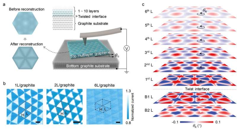
(a) A schematic of the experimental setup. (b) Typical current images measured on samples with twisted interface embedded in different depths. (c) Maps of the atomic deformation in individual graphene layers calculated by molecular calculations. Credit: Science China Press

To answer these questions, Professor Qunyang Li’s group at Tsinghua University and Professor Ouyang Wengen’s group at Wuhan University have developed a new method based on conductive atomic force microscopy (c-AFM) to characterize and reconstruct the internal stacking state of twisted layered material through simple surface conductivity measurements. The related work has been published in National Science Review.

See also  A theoretical approach to ferroelectricity in hafnia-related materials

Their experimental results have shown that the twisted interfaces can still undergo atomic reconstruction and notably affect the surface conductivity even when they are embedded 10 atomic layers beneath the surface. To better understand the atomic structure of the twisted multilayer system, a multilayer graphene system similar to the experimental samples has been constructed in a molecular dynamics (MD) simulation model by accurately considering the interlayer interactions.

The simulation results have revealed that for small-angle twisted interfaces embedded in the interior of material, atomic reconstruction can indeed occur and promote the in-plane rotational deformation of the adjacent graphene layers. However, the atomic rotational deformation of graphene layer gradually decays as one moves away from the twisted interface.

Based on the atomic structures revealed in MD simulations, the research group proposed a series spreading resistance model (SSR model) to quantify the influence of the stacking state of twisted multilayer system on its surface conductivity.

The new model enables a correlation between the surface conductivity and the internal stacking structure to be made directly, which is applicable even for twisted multilayer samples with complex crystal defects (e.g., dislocations). The work provides a simple, convenient and high-resolution means to characterize the internal stacking structures of twisted layered materials, which is crucial for fundamental studies of 2D stacked structures and the development of emerging twisted electronics.

Provided by
Science China Press


Source link

embedded interfaces materials Twisted TwoDimensional Visualizing
Share. Facebook Twitter Pinterest LinkedIn Tumblr Email

Related Posts

2D hybrid material integrates graphene and silica glass for next-generation electronics

June 4, 2025

Zeolite nanopore model links crystal size to metal cluster migration and catalyst performance

June 4, 2025

Spontaneous symmetry breaking in electron systems proves elusive

June 3, 2025

Improving Crop Tolerance to Drought and Heat Using Nanomaterials

June 3, 2025

Crystal-modifying agent piracetam provides scalable strategy for high-efficiency all-perovskite tandem solar cells

June 3, 2025

Phonon decoupling in naturally occurring mineral enables subatomic ferroelectric memory

June 2, 2025

Comments are closed.

Top Articles
Medical

Novel bottom-up approach in synthetic immunology opens a new frontier for disease treatment

News

A History of the Semiconductor Chip

Logical operations using RNA droplets

Editors Picks

2D hybrid material integrates graphene and silica glass for next-generation electronics

June 4, 2025

Zeolite nanopore model links crystal size to metal cluster migration and catalyst performance

June 4, 2025

Spontaneous symmetry breaking in electron systems proves elusive

June 3, 2025

Improving Crop Tolerance to Drought and Heat Using Nanomaterials

June 3, 2025
About Us
About Us

Your go-to source for the latest nanotechnology breakthroughs. Explore innovations, applications, and implications shaping the future at the molecular level. Stay informed, embrace the nano-revolution.

We're accepting new partnerships right now.

Facebook X (Twitter) Instagram Pinterest
Our Picks

New Power Generator Produces Continuous Electricity From Natural Atmospheric Humidity

September 22, 2023

Studying thin films under extreme temperatures with reflectometry

July 6, 2024

Exploring the green power of fungi

September 19, 2023

Subscribe to Updates

Get the latest creative Nano Tech news from Elnano.com

© 2025 Elnano.com - All rights reserved.
  • Contact
  • Privacy Policy
  • Terms & Conditions

Type above and press Enter to search. Press Esc to cancel.

Cleantalk Pixel