


Researchers from Kyushu University and Nitto Denko have developed tape that changes its ‘stickiness’ to 2D materials due to UV light. Credit: Ago Lab, Kyushu University
Researchers create UV-sensitive tape that can transfer 2D materials like graphene in an easier, cheaper, and less damaging way.
Materials just atoms in thickness, known as two-dimensional (2D) materials, are set to revolutionize future technology, including in the electronics industry. However, the commercialization of devices that contain 2D materials has faced challenges due to the difficulty in transferring these extremely thin materials from where they are made onto the device.
Breakthrough in 2D Material Transfer
Now, a research team from Kyushu University, in collaboration with Japanese company Nitto Denko, has developed a tape that can be used to stick 2D materials to many different surfaces, in an easy and user-friendly way. Their findings were published in Nature Electronics on February 9, 2024.
“Transferring 2D materials is typically a very technical and complex process; the material can easily tear, or become contaminated, which significantly degrades its unique properties,” says lead author, Professor Hiroki Ago of Kyushu University’s Global Innovation Center. “Our tape offers a quick and simple alternative, and reduces damage.”
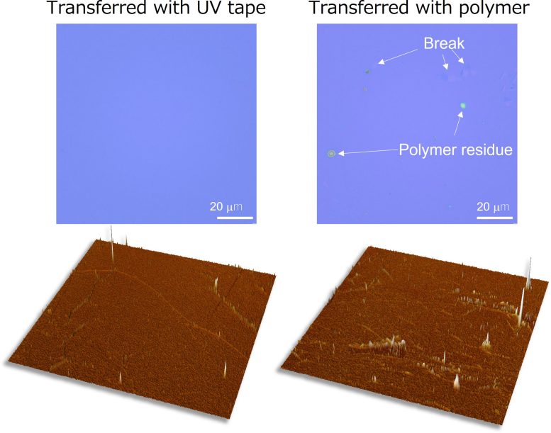
Researchers from Kyushu University showed that using UV tape to transfer graphene instead of polymer better maintained the material’s integrity and reduced defects. Credit: Ago Lab, Kyushu University
Enhancing the Application of Graphene
The researchers began by focusing on graphene. Made from a thin sheet of carbon atoms, graphene is tough, flexible, and light, with high thermal and electrical conductivity. Dubbed a “wonder material” upon discovery, it has potential applications in biosensing, anti-cancer drug delivery, aeronautics, and electronic devices.
“One of the main methods of making graphene is through chemical vapor deposition, where graphene is grown on copper film. But to perform properly, the graphene must be separated from the copper and transferred onto an insulating substrate, like silicon,” Professor Ago explains. “To do this, a protective polymer is placed over the graphene, and the copper is then removed using etching solution, such as acid. Once attached to the new substrate, the protective polymer layer is then dissolved with a solvent. This process is costly, time-consuming, and can cause defects to the graphene’s surface or leave traces of the polymer behind.”
Professor Ago and his colleagues therefore aimed to provide an alternative way of transferring graphene. They used AI to develop a specialized polymer tape, dubbed “UV tape,” which changes its attraction to graphene when irradiated with UV light.
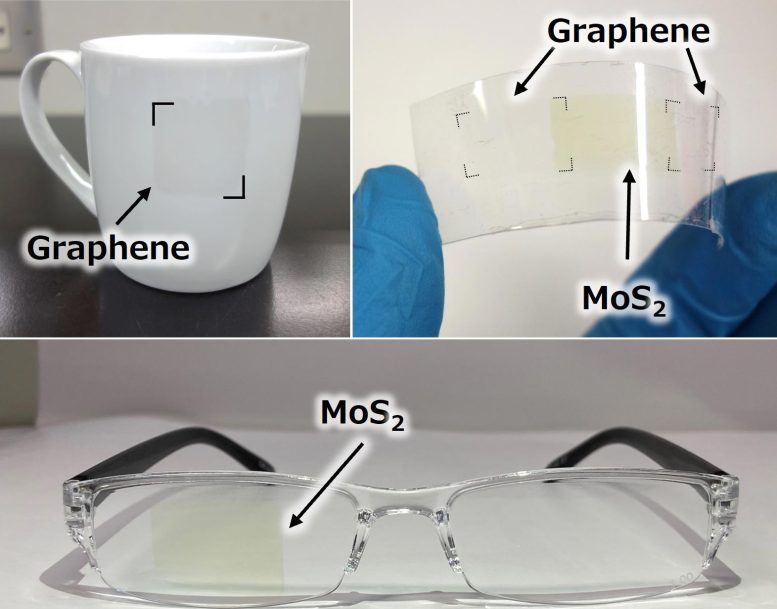
The newly designed UV tape is able to transfer 2D materials, including graphene and transition metal dichalcogenides, onto a range of different substrates, including silicon, ceramic, glass and plastic. Credit: Ago Lab, Kyushu University
Advancing 2D Materials With UV Tape
Before exposure to UV light, the tape has a strong adhesion to graphene, allowing it to “stick.” However, after UV exposure, the atom bonding changes, which decreases the level of adhesion to graphene by about 10%. The UV tape also becomes slightly stiffer and easier to peel off. Taken together, these changes allow the tape to be peeled off the device substrate while leaving the graphene behind.
The researchers also developed tapes that can transfer two other 2D materials: white graphene (hBN), an insulator that can act as a protective layer when stacking 2D materials, and transition metal dichalcogenides (TMDs), a promising material for the next generation of semiconductors.
Importantly, when the researchers looked closely at the surface of the 2D materials after transfer, they saw a smoother surface with fewer defects than when transferred using the current conventional technique. Upon testing the materials’ properties, they also found that they were more efficient.
Researchers from Kyushu University and Nitto Denko have so far succeeded in transferring wafers of graphene up to 10 cm in diameter using UV tape. With smaller pieces of UV tape, the sticking and peeling can be done by hand. However, machines are useful when scaling up for mass production. Credit: Nakatani et al. Nature Electronics, https://doi.org/10.1038/s41928-024-01121-3
Transfer using UV tape also offers numerous other advantages over current transfer techniques. Because the UV tape is bendy, and the transfer process doesn’t require the use of plastic-dissolving solvents, flexible plastics can be used as the substrate of the device, expanding potential applications.
“For example, we made a plastic device that uses graphene as a terahertz sensor. Like X-rays, terahertz radiation can pass through objects that light can’t, but doesn’t damage the body,” Professor Ago says. “It’s very promising for medical imaging or airport security.”
What’s more, the UV tape can be cut to size so that only the exact amount of 2D material needed is transferred, minimizing waste and reducing cost. 2D layers of different materials can also be easily laid on top of each other in different orientations, allowing researchers to explore new emerging properties from the stacked materials.
Expanding and Simplifying the Use of 2D Materials
For their next steps, the researchers are aiming to expand the size of the UV tape to the scale needed for manufacturers. Currently, the largest wafer of graphene that can be transferred is 10 cm in diameter. Professor Ago and his colleagues are also trying to resolve the problem of wrinkles and bubbles that form on tape, causing small defects.
The research team also hope to improve stability, so that 2D materials can be attached to UV tapes for a longer period of time, and distributed to end users, such as other scientists.
“The end users can then transfer the material onto their desired substrate by applying and removing the UV tape like a child’s sticker, with no training needed,” says Professor Ago. “Such an easy method could fundamentally change the style of research and accelerate the commercial development of 2D materials.”
Reference: “Ready-to-transfer two-dimensional materials using tunable adhesive force tapes” 9 February 2024, Nature Electronics.
DOI: 10.1038/s41928-024-01121-3
