


Two-dimensional (2D) materials, including semi-metallic graphene, semiconducting transition metal dichalcogenides (TMDs), and insulating hexagonal boron nitride (hBN), have been a hot topic in recent years due to their potential as electrically or photonically innovative materials.
Image Credit: ShutterStock/artbase
In the realm of electronic devices, particularly in the domain of memory devices, significant research has centered around non-volatile floating gate transistors. These transistors are explored as effective means for high-performance information storage.1,2
Van der Waals (vdW) heterostructures composed of 2D materials have also been a topic of interest due to their ability to function as artificial synaptic emulators in neuromorphic computing systems.2,3
In this regard, the typical 2D materials-based floating gate memories are constituted from TMDs, hBN, and graphene as semiconductors, tunnel barriers, and floating gates, respectively. Thus, understanding the fundamental factors that influence charge trapping or de-trapping within deep potential wells is crucial.
Consequently, a thorough investigation into the energy level properties of 2D materials becomes imperative to establish the efficiency of rapid and energy-efficient flash memories.
For this, a floating gate memory structure was fabricated using mechanically exfoliated thin MoS2, hexagonal boron nitride (hBN), and multilayer graphene (MLG). Afterward, an assessment of the work functions of these distinct layers was carried out based on the back-gate voltages using a kelvin probe force microscopy (KPFM) apparatus.
Materials and Methods
Transfer Process for 2D Materials
Flakes of each 2D material (MoS2, hBN, and MLG) were exfoliated onto a rectangular piece of cured polydimethylsiloxane (PDMS) using the standard scotch tape method.4
Following this, the exfoliated 2D materials were transferred onto the SiO2/p++Si substrate in the MoS2/hBN/MLG stacking sequence. During the transfer process, precise alignment of the 2D flakes on PDMS was achieved using a micro-manipulator, ensuring accurate placement on the target substrate before coming into contact.
KPFM Measurement with Gate Bias
KPFM measurements were conducted using a commercial atomic force microscope system (NX10, Park Systems Corp.) at room temperature in air.
A conductive tip consisting of an Au-coated cantilever with a Cr sublayer on an n-type silicon material (manufactured by Mikromash Corp., spring constant: 1 N/m, resonance frequency: 90 kHz) was employed.
For surface potential observation, an AC voltage amplitude of approximately 2 V and a frequency of 17 kHz was applied to the conductive probe.
The surface potential was derived by applying a DC voltage (VDC) via a lock-in amplifier to nullify the electrostatic force between the Au-coated tip and the sample resulting from the AC voltage (VAC) applied to the tip.5,6
To study the impact of back-gate bias (VBG) during KPFM analysis, changes in surface potential were monitored while maintaining a constant VBG bias. This involved sequentially applying a VBG of either 0 V or 40 V.
Morphology and surface potential data was subsequently analyzed using Park Systems XEI software to extract numerical information from the acquired mapping images.
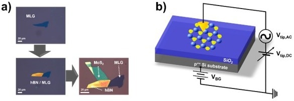
Figure 1. a) Optical microscope images of the transfer process for 2D vdW heterostructures (MoS2/hBN/MLG). b) Representative schematic of the KPFM setup with applied VBG for the 2D materials on a SiO2/Si substrate. The scale bars in a) are 20 µm.
Image Credit: Park Systems
Results and Discussion
To create multi-stacked 2D heterostructures, researchers sequentially transferred MLG, hBN, and MoS2 onto a SiO2/p++Si substrate, as displayed in Figure 1a. These transferred materials were chosen for their roles: MLG acts as a semi-metal, hBN as a wide bandgap insulator, and MoS2 as a semiconductor.
The multi-stacked heterolayers were examined using the KPFM setup, with applied VBG to study how surface potentials change in each 2D layer based on back-gated voltages, as shown in Figure 1b.
The system allowed for the adjustment of Fermi levels or work functions via back-gate bias. The successful construction of the multi-stacked heterostructure was confirmed through optical microscopy, as presented in Figure 2a.
Importantly, the transfer process left the layer surfaces mostly uncontaminated, preserving topographical and electrical information.
By analyzing a line-scan height profile from the AFM morphology image, researchers calculated approximate thicknesses of MoS2, hBN, and MLG, resulting in values of 6.9, 60.5, and 12.0 nm, respectively. This stacking arrangement, along with the thickness values for each of the three layers, is illustrated in Figure 2d.

Figure 2. a) Optical image of MoS2/hBN/MLG heterostructure. The scale bar in a) is 10 µm. b) A surface topography image of a). The scale bar in b) is 5 µm. c) The height profile of the line-scan (blue dash line) indicated in b). d) The stacked multi-layer heterostructure on a SiO2 substrate with the respective thickness values as measured in c).
Image Credit: Park Systems
To validate the distinct behavior of MoS2-based floating gate memory devices, the team employed a KPFM system to measure surface potentials and work functions of MoS2, hBN, and MLG. VBG was applied, as seen in Figures 3a, 3b, 3d, and 3e, for each material, respectively.
KPFM measurements provided the contact potential difference (VCPD) between the AFM tip coated with Au and the sample, leading to the derivation of the following relationship.
| eVCPD = WFtip — WFsample ⇒ WFsample = WFtip — eVCPD | (1) |
where WFsample and WFtip are the work functions of the sample and tip, respectively, and e is the electronic charge. Given that the van der Waals heterostructure rests on a SiO2 substrate, researchers used the contact potential and work function of MLG as reference points.
As a result, differences in contact potential or work function between the various multi-stacked layers and MLG can be expressed through the provided equations below.
| △VCPD (hBN / MLG) = VCPD (hBN / MLG) — VCPD (MLG) ≡ △VH – G | (2) |
| △WF(hBN / MLG) = WF(hBN / MLG) — WF(MLG) ≡ △WFH – G | (3) |
For the MoS2/hBN/MLG stacking layers,
| △VCPD (MoS2 / hBN / MLG) = VCPD (MoS2 / hBN / MLG) — VCPD (MLG) ≡ △VM – G | (4) |
| △WF(MoS2 / hBN / MLG) = WF(MoS2 / hBN / MLG) — WF(MLG) ≡ △WFM – G | (5) |
The work-function difference (ΔWFH-G or ΔWFM-G) was calculated through equation (3) for hBN or equation (5) for MoS2.
As observed in Figures 3c and 3f, when a bias of 40 V was applied to the voltage back-gate (VBG), the Fermi energy levels of the two stacked 2D materials (MoS2 and hBN) shifted higher from their initial positions (at VBG = 0 V), relative to the work-function level of monolayer graphene (MLG).
In the case of ‘VBG = 0 V’, the differences in work function for the two surfaces, hBN/MLG (ΔWFH-G), and MoS2/hBN/MLG (ΔWFM-G) layers were approximately -171.9 meV and -265.8 meV, respectively.
This positioning situated the Fermi levels below the MLG’s work function level. However, under the condition of ‘VBG = 40 V’, the work-function differences for the hBN/MLG (ΔWFH-G) and MoS2/hBN/MLG (ΔWFM-G) layers were around 89.0 meV and 125.2 meV, respectively.
Hence, the Fermi levels are positioned higher than the MLG work function level.
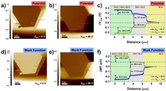
Figure 3. KPFM images of multilayer vdW heterostructure (MoS2/hBN/MLG): a, b) surface potential and d, e) work function in the case of VBG = 0 V (a, d), or VBG = 40 V (b, e). Line scan profiles of potential (c), and work function (f), which are indicated in a, b), and d, e), respectively. The scale bars in a, b, d, e) are 5 µm.
Image Credit: Park Systems
Due to the differing work-function behaviors depending on the VBG bias, the MLG layer could be effectively charged with electrons or holes through tunneling. In summary, under a VBG bias of 0 V, electrons within the MLG layer could migrate more easily to the MoS2 layer by overcoming the barrier of the hBN layer.
Contrary to this, for the VBG condition of 40 V, the MLG layer would be convenient for obtaining electrons from the MoS2 layer with a reduced energy barrier between the MoS2 and hBN layers.
Conclusion
The study of charge transfer behavior through the insulating hBN layer employed the back-gated Kelvin Probe Force Microscopy (KPFM) mode. This method investigated the surface potential properties of 2D materials under back-gate voltages of 0 and 40 V.
The reasons for the charging and discharging behavior of graphene layers within the MoS2/hBN/MLG structure on SiO2/p++Si substrate were examined via the back-gated KPFM method.
Ultimately, the back-gated KPFM method could be widely employed to characterize the device operation mechanisms of non-volatile floating gate memories, memtransistors, and various other electrically functional devices.
References
- Bertolazzi, S.; Bondavalli, P.; Roche, S.; San, T.; Choi, S. Y.; Colombo, L.; Bonaccorso, F.; Samori, P., Nonvolatile Memories Based on Graphene and Related 2D Materials. Adv Mater 2019, 31 (10), e1806663.
- Seo, S.; Lee, J. J.; Lee, H. J.; Lee, H. W.; Oh, S.; Lee, J. J.; Heo, K.; Park, J. H., Recent Progress in Artificial Synapses Based on Two-Dimensional van der Waals Materials for Brain-Inspired Computing. Acs Appl Electron Ma 2020, 2 (2), 371-388.
- Yi, S. G.; Park, M. U.; Kim, S. H.; Lee, C. J.; Kwon, J.; Lee, G. H.; Yoo, K. H., Artificial Synaptic Emulators Based on MoS2 Flash Memory Devices with Double Floating Gates. ACS Appl Mater Interfaces 2018, 10 (37), 31480-31487.
- Huang, Y.; Sutter, E.; Shi, N. N.; Zheng, J.; Yang, T.; Englund, D.; Gao, H. J.; Sutter, P., Reliable Exfoliation of Large-Area High-Quality Flakes of Graphene and Other Two-Dimensional Materials. ACS Nano 2015, 9 (11), 10612-20.
- Yu, Y. J.; Choe, J. H.; Kim, J. Y.; Gwon, O. H.; Choi, H. K.; Choi, J. S.; Kim, J. H.; Kim, J. S.; Kim, J. T.; Shin, J. H.; Choi, Y. K., Gate-tuned conductance of graphene-ribbon junctions with nanoscale width variations. Nanoscale 2019, 11 (11), 4735-4742.
- Yu, Y. J.; Zhao, Y.; Ryu, S.; Brus, L. E.; Kim, K. S.; Kim, P., Tuning the graphene work function by electric field effect. Nano Lett 2009, 9 (10), 3430-4.

This information has been sourced, reviewed and adapted from materials provided by Park Systems.
For more information on this source, please visit Park Systems.
