


The photomask plays a critical role in photolithography for creating patterns on semiconductor wafers during manufacturing. It selectively transmits or reflects light to form patterns on the target substrate.
Image Credit: ShutterStock/IM Imagery
Defects on the photomask can arise from absorber patterning or during mask handling, potentially compromising wafer quality and the functionality of the final device.
Various repair methods, such as E-beam, ion, laser, and nano machining techniques, are conventionally used to address these issues. Atomic force microscopy (AFM) images surfaces using a sharp tip of several or tens of nanometers.
AFM is widely used in the semiconductor industry as well as the materials, chemical, electrical, electronic, and biological industries. In the semiconductor sector, AFM’s high precision and accuracy have become increasingly crucial for tasks like metrology and failure analysis.
The trend towards smaller-scale processes has also led to a greater demand for AFM as a tool for rectifying defects. Capitalizing on this trend, AFM’s capability for non-destructive, high-precision imaging is being applied to repair photomasks.
This article discusses the transition of the AFM tip from surface imaging to the targeted removal of photomask defects, effectively restoring the photomask’s original functionality.
Park Systems is at the forefront of this technological advancement with the introduction of the NX-Mask automated AFM. This article explores the concept of photomask repair using Park Systems’ NX-Mask and provides real-world examples of its various applications.
Park Systems NX-Mask
The NX-Mask is an automated AFM developed for photomask repair (as shown in Figure 1). It uses an AFM tip to remove defects while maintaining the sample surface’s integrity. Due to its automated nature, the NX-Mask can accurately eliminate nanometer-sized defects during mask repair.
It can also analyze sample surfaces at a sub-nanometer scale, including measuring surface roughness and pattern dimensions. This versatility allows for various sample studies beyond mask repair.

Figure 1. Park Systems NX-Mask.
Image Credit: Park Systems
Mask Repair Process
For photomask repair, the NX-Mask employs a single-crystal diamond tip, enabling effective defect removal and prolonged tip life. The repair process involves three main steps:
1) Survey scanning
2) Repair (defect removal)
3) Post-repair imaging (illustrated in Figure 2)
During the survey scan, the defect’s precise location and size are determined with nanometer-level accuracy. Once identified, the NX-Mask uses the AFM tip to eliminate the defect.
Subsequently, the post-repair imaging step confirms the success of the defect removal process. Real-time AFM results allow continuous monitoring of each stage, with defect removal being validated by comparing the survey scan with the post-repair images.
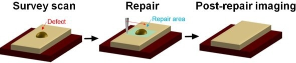
Figure 2. Photomask repair process on the NX-Mask.
Image Credit: Park Systems
Mask Repair Examples On the Park Systems NX-Mask
Photomask repair on the NX-Mask system involves two main categories based on the substrate material and defect nature: 1) soft defect and 2) hard defect. These categories follow the same basic photomask repair sequence outlined earlier but with minor differences tailored to the defect type.
The first example, shown in Figure 3, demonstrates a soft defect repair within a photomask pattern. The initial image on the left displays the survey scan results, clearly revealing the defect within the pattern.
After the defect removal step, the post-repair image on the right confirms the successful defect elimination.
Moreover, due to the non-destructive nature of AFM, it can be confirmed that the photomask pattern is maintained through a comparison of the survey scan and the post-repair imaging, which shows that only defects are selectively removed without any damage to the mask surface.
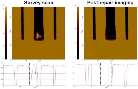
Figure 3. Soft defect repair on photomask.
Image Credit: Park Systems
In another instance of soft defect repair, a defect measuring around 200 nm in height was removed from the photomask pattern (Figure 4). The defect was identified through the survey scan and then selectively addressed during the repair step.
It is worth noting that in the repair image of Figure 4, a residue of the defect remains at the base of the pattern.
This partial removal simplifies its elimination in an additional repair step, as shown in the post-repair imaging. Here, all defects in the pattern were completely removed through the repeated repair process.
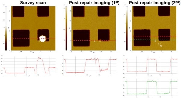
Figure 4. Soft defect repair on photomask. Here, repetitive defect removal steps were required to eliminate the defect.
Image Credit: Park Systems
Figure 5 presents the outcome of a hard defect repair involving material removal within the photomask material itself. The mask repair procedure follows a similar process to the soft defect case, with the distinction being the progressive scratching of the defect site using the AFM tip while preserving the photomask pattern.
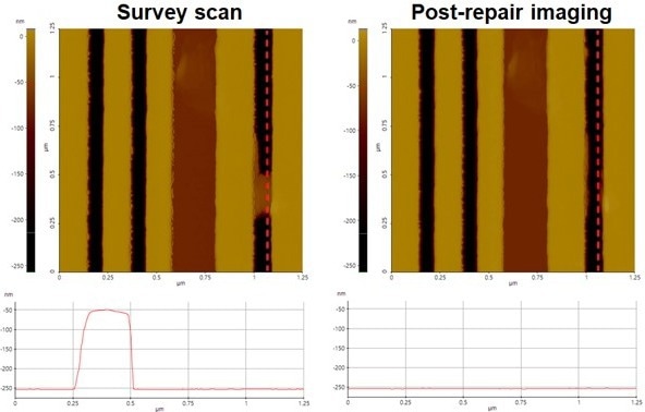
Figure 5. Hard defect mask repair.
Image Credit: Park Systems
Conclusion
This article highlights the NX-Mask system‘s ability to repair masks for both soft and hard defects.
The sequential approach of Survey scan/ Repair/Post-repair imaging enables accurate defect identification and selective removal or relocation on the photomask surface without compromising its integrity, as confirmed by the final post-repair imaging.
The application of AFM extends beyond surface measurements in the semiconductor industry, with mask repair by the Park Systems NX-Mask system offering a versatile solution for AFM that can keep pace with the increasingly challenging demands of photolithography in the semiconductor industry.

This information has been sourced, reviewed and adapted from materials provided by Park Systems.
For more information on this source, please visit Park Systems.
