


Frequently used as their primary power source, lithium-ion batteries (LIBs) are key components of modern electronics1-3. Understanding the mechanical and electrical properties of electrode materials plays a key role in the performance enhancement of LIBs.
Research using PinPoint™ SSRM is provided in this article to measure both electrical and mechanical properties of LIB electrode surfaces effectively, at a much higher quality in a high vacuum environment than in ambient conditions.
The data that was gathered in this experiment shows that this method is an effective means for measuring the quantitative and qualitative topographical, electrical and mechanical data of advanced materials with enhanced data accuracy and image quality.
Introduction
LIBs are ubiquitous in a number of applications ranging from electric vehicles to portable devices because of their flexible and lightweight design, high energy density, low cost, low self-discharge, and long lifespan when compared to other battery technologies4,5.
The reliability and performance of LIBs must still be improved in order to meet the requirements of applications like large-scale energy storage and hybrid electric vehicles (HEVs) despite all of these benefits2,5.
Extensive research has focused on the development of four cell materials to acquire better performance; 1) positive and 2) negative electrode active materials (AM), 3) separators, and 4) electrolytes2. Understanding the electrical and mechanical properties of electrode materials plays a key part in the performance improvement of LIBs.
It has been determined that better adhesion between electrode films, electrode particles, and current collectors results in better retention of discharge capacity during cycling, particularly when electrode materials show faster and/or larger volume expansion2.
Furthermore, enhanced electronic conductivity and ionic diffusion in electrodes also results in LIB capacity improvement6. Optimizing electrical and mechanical properties on a nanometer scale has become more relevant leading to improved interfaces, as devices have become more compact.
There are a number of techniques which can measure these local properties. The more common techniques include impedance spectroscopy and nanoindentation3,7,8. Yet, one cannot get the full local information about the aforementioned properties, even using both techniques.
Impedance spectroscopy only distinguishes between interfaces and requires an exact model. So, it does not give local information for each interface. Nanoindentation is destructive and does not supply any electrical information.
Scanning Spreading Resistance Microscopy (SSRM) is one of the more effective tools utilized to overcome the problems encountered in electrical property measurement. This method measures both electrical properties and topography simultaneously.
SSRM is an implementation of a well-established Spreading Resistance Profiling (SRP) technique employed for micro- and nano-scale. The operation of Conductive-AFM and SSRM is identical except that SSRM scans the cross-sectioned surface of a device, while in Conductive-AFM a generalized surface is scanned.
The applications of SSRM include establishing the dopant distribution in semiconductor materials in addition to exact pn-junction delineation.
Yet, SSRM has some drawbacks, like degradation of image resolution, fast wearing of the tip, and low signal-to-noise ratio. These drawbacks come from the high frictional force arising from continuous tip-sample contact during scanning.
A new operational atomic force microscopy (AFM) mode recently developed by Park Systems called PinPoint™10 has been coupled with SSRM to provide engineers and scientists with an innovative solution to avoid the troublesome frictional forces during a scan.
To ensure frictionless operation, PinPoint™ operates in an approach-retract manner. This stops the lateral force from continuous tip-sample contact. Furthermore, the integration of these techniques with AFM allows the simultaneous acquisition of topography and electrical/mechanical property data without changing the sample or tip.
Here, it is shown that PinPoint™ SSRM measures both mechanical and electrical properties of LIB electrode surfaces effectively, at a much higher quality in a high vacuum environment than in ambient conditions with a Park NX-Hivac AFM system.
Materials and Methods
A Park NX-Hivac AFM system was utilized to examine An LIB electrode9. The mechanical (stiffness and adhesion), topographical, and electrical (resistance and conductance) data of the sample were measured under high-vacuum (10-5 torr range) to carry out a 20 µm x 12 µm scan with a resolution of 256 x 150 pixels.
For this experiment a conductive diamond coated probe (NANOSENSORS™ CDT-NCHR) with a nominal force constant of 80 N/m was utilized. In PinPoint™ SSRM the electrical properties, topography, and mechanical properties of a sample can be gathered at the same time.
By monitoring its feedback signal the conductive tip maps the topography and approaches the sample until it reaches a predefined force threshold point. Next, it measures the Z scanner height and retracts rapidly.
Each time the tip engages the sample surface the current distribution of the samples is mapped. The current flow, generated by the applied bias voltage between the conductive tip and sample, is measured at each landing point to acquire the electrical data.
Typically, the current flow is very small and must be augmented by a current amplifier before it can be processed into an image. The Park NX-Hivac supports the utilization of an internal current amplifier with a variable gain of 106~1012 V/A which is applicable to most measurements.
In this experiment the applied external sample bias used was 3V. Furthermore, at each point of the image, the force-distance curve was gathered and utilized to calculate the mechanical properties of the sample being measured.
The XY scanner stops during data acquisition, and the contact time is controlled to allow enough time for the scanner to gather accurate and precise data. All of the images were analyzed using Park XEI software which drew a corresponding line profile and carried out the image analysis.
Results and Discussion
Performing this experiment under high-vacuum resulted in the increase in sensitivity and resolution measurements when compared to the employment of other methods9. High-vacuum also led to higher repeatability and accuracy while minimizing damage suffered by the tip and/or sample.
When compared to experiments conducted in ambient air or N2 the applied force between the tip and sample under high-vacuum can be much lower since the residual thin liquid film, which is always present under ambient conditions, decreases the quality of the electrical contact9.
Figures 1 and 2 show the quantitative and qualitative results gathered during these experiments Figure 1 shows the topography and electrical data measured in the sample. The topography image (Fig. 1A) shows that the sample surface is made up of circular shaped plateaus with diameters ranging from 2 to 8 µm.
Figure 1. Topography (Fig. 1A), resistance (Fig. 1B), and conductance (Fig. 1C) image acquired from a LIB electrode sample. Line profile (Fig. 1D): Topography line profile (red line, y-axis on left), resistance line profile (green, y-axis on right), and conductance line profile (blue line, y-axis on right). 3D-overlay image of topography and conductance (Fig. 1E).
The circular plateaus with darker color represent low lying areas and the brighter colors represent areas with greater height. The resistance image (Fig. 1B), features brighter colored areas which represent higher surface resistivity while areas with darker colors represent lower surface resistivity.
The brighter colors on the conductance image (Fig. 1C) represent higher conductivity while the darker colors represent areas with lower surface conductivity. When comparing topography and resistance images, it can be determined that when compared to low lying areas, higher circular plateaus have lower resistance.
A comparison of the topography and conductance images shows that circular plateaus with higher height have higher conductance when compared to low lying areas. This can also be seen in the 3D-overlay image of topography and conductance (Fig. 1D) gathered in the XEI mode.
Both conductance and resistance images show a clear picture of the small grains surrounding the circular plateaus. It was found that these small grains have higher conductivity and lower resistivity when compared to the circular plateaus.
Examination of the corresponding line profile (Fig. 1E) of the conductance, topography, and resistance images confirms that the circular plateaus are regions with the highest height (approximately 50-60 nm).
Low lying areas, on the other hand, possess the highest resistivity (around 8 GΩ). The line profile of the conductance image demonstrates that the small grains around the circular plateaus are regions with the highest conductivity (around 1.3 µS).
The mechanical data measured from the sample is shown in Figure 2. In the stiffness images, the darker areas correspond to the surface with lower stiffness and modulus, while the brighter areas represent a surface with higher stiffness and modulus.
The adhesion image does not exhibit significant variations between the plateaus. A tendency towards higher adhesion is seen between the plateaus. The average adhesion force was calculated to be 80 nN. Noticeable stiffness variations in the sample surface are shown in the stiffness image.
Represented by the dark color map, the measured stiffness value of the circular features was around -2.8 µV (note that the stiffness unit given here is qualitative data for comparative purposes and does not represent an absolute physical unit value of stiffness), while the areas represented by the bright color map were between -1.5 and -2.0 µV.
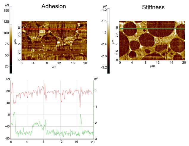
Figure 2. Adhesion (Fig. 2A) and stiffness images (Fig. 2B) acquired from a LIB electrode sample. Line profile (Fig. 2C): Adhesion line profile (red line, y-axis on left) and stiffness line profile (green, y-axis on right).
Conclusion
The Park NX-Hivac system using Pinpoint™ SSRM successfully characterized a lithium-ion battery electrode.
The data which was gathered in this experiment shows that this method is an effective way to measure the quantitative and qualitative electrical, topographical, and mechanical data of advanced materials with improved data accuracy and image quality.
Overall, the PinPoint™ method utilized in this study will help researchers and device engineers greatly in understanding the mechanical and electrical behavior of certain materials with unique properties, like LIB electrodes.
References and Further Reading
- J-M Tarascon and M Armand, Nature 414(6861) (2001) 359-67.
- J Chen, J Liu, Y Qi, T Sun, and X Li, Journal of The Electrochemical Society 160(9) (2013) A1502-A1509.
- L Vasconcelos, R Xu, J Li, and K Zhao, Extreme Mechanics Letters 9(3) (2016) 495-502.
- G Kermani and E Sahraei, Energies 10(11) (2017) 1730.
- A Mishra, A Mehta, S Basu, S Malode, N Shetti, S Shukla, M Nadagouda, and T Aminabhavi, Materials Science for Energy Technologies 1(2) (2018) 182-187.
- M Park, X Zhang, M Chung, G Less, and A Sastry, Journal of Power Sources 195(24) (2010) 7904-7929.
- Y Gao, M Cho, and M Zhou, Journal of Mechanical Science and Technology 27(5) (2013) 1205-1224.
- E Reinholz, S Roberts, C Apblett, J Lechman, and P Schunk, Journal of The Electrochemical Society 163 (8) (2016) A1723-A1729.
- Park Systems Inc. (2015, May 6). Park Systems Introduces Park NX-Hivac, a High Vacuum SSRM AFM System for Optimal Results in Semiconductor Manufacturing Failure Analysis [Web Post]. Retrieved from https://parksystems.com/company/news/press-release/480-park-nx-hivac-a-high-vacuum-ssrm-afm-system
- JP Pineda, C Newcomb, G Pascual, B Kim, and K Lee (2017, May 1). Optimum Current Distribution Measurement of Zinc Oxide Nanorods via PinPoint™ Conductive AFM [Online Article]. Retrieved from https://parksystems.com/images/media/appnote/Optimum-Current-Distribution-Measurement-of-Zinc-Oxide-Nanorods-via-PinPoint-Conductive-AFM_20.pdf
- F Susai, H Sclar, Y Shilina, T Penki, R Raman, S Maddukuri, S Maiti, I Halalay, S Luski, B Markovsky, and D Aurbach, Advanced Materials 30(41) (2018) 1801348.
Acknowledgments
Produced from materials originally authored by John Paul Pineda, Cathy Lee, Byong Kim, and Keibock Lee from Park Systems Inc.
This information has been sourced, reviewed and adapted from materials provided by Park Systems.
For more information on this source, please visit Park Systems.
