Close Menu
  • News
  • Medical
  • Technology
  • Nanomaterials
  • Research
  • Blog
    • Nasiol.com
  • Contact
    • Tech7685@gmail.com
What's Hot

Finely-tuned TiO₂ nanorod arrays enhance solar cell efficiency

May 28, 2025

Different DLS-Based Systems Can Give Us Different Size Results

May 27, 2025

2D Janus heterobilayers lead the way

May 27, 2025
Facebook X (Twitter) Instagram
Nanotech – Nanomaterials | Medical | Research | News Stories Updated Daily Nanotech – Nanomaterials | Medical | Research | News Stories Updated Daily
  • News
  • Medical
  • Technology
  • Nanomaterials
  • Research
  • Blog
    • Nasiol.com
  • Contact
    • Tech7685@gmail.com
Facebook X (Twitter) Instagram
Nanotech – Nanomaterials | Medical | Research | News Stories Updated Daily Nanotech – Nanomaterials | Medical | Research | News Stories Updated Daily
Home»News»Ultrafast plasmon-enhanced magnetic bit switching at the nanoscale
News

Ultrafast plasmon-enhanced magnetic bit switching at the nanoscale

May 6, 2025No Comments4 Mins Read
Facebook Twitter Pinterest Telegram LinkedIn Tumblr WhatsApp Email
Ultrafast plasmon-enhanced magnetic bit switching at the nanoscale
Share
Facebook Twitter LinkedIn Pinterest Telegram Email
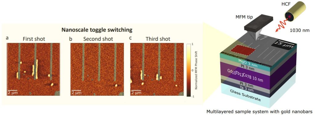
Schematic illustration of direct in-situ high-resolution magnetic imaging using MFM. An ultrashort intense laser pulse is guided through a hollow-core fiber and applied to plasmonic structures deposited on a magnetic multilayer sample. The change in magnetic state probed after irradiation of (a) First laser shot focused on the plasmonic nanobars (superimposed in green). (b) Second laser shot with the same fluence switches the magnetization state back to its original state. (c) Excitation with the third laser pulse reverses the magnetization state at the edge of the nanobars. Credit: MBI: T.P.H. Sidiropoulos, P. Singh

Researchers from Max Born Institute have demonstrated a successful way to control and manipulate nanoscale magnetic bits—the building blocks of digital data—using an ultrafast laser pulse and plasmonic gold nanostructures. The findings were published in Nano Letters.

All-optical, helicity-independent magnetization switching (AO-HIS) is one of the most interesting and promising mechanisms for this endeavor, where the magnetization state can be reversed between two directions with a single femtosecond laser pulse, serving as “0s” and “1s” without any external magnetic field or complex wiring. This opens up exciting possibilities for creating memory devices that are not only faster and more robust but also consume far less power.

Ultrafast light-driven control of magnetization on the nanometer-length scale is key to achieving competitive bit sizes in next-generation data storage technology. However, it is currently not well understood to what extent basic physics processes such as heat transfer at the nanoscale and the propagation of magnetic domain walls limit the minimum achievable bit size.

To investigate these open questions, the researchers used plasmonic gold nanostructures, which can confine light to regions smaller than the wavelength of light. These structures were fabricated in-house by electron beam lithography on a 10 nm thin film of a magnetic material composed of rare earth—transition metal alloy (GdTbCo), capable of facilitating small stable magnetic domains due to the presence of the rare earth metal terbium, generating a large magnetic anisotropy.

  • Ultrafast plasmon-enhanced magnetic bit switching at the nanoscale
    All optical switching from off- and on-resonant nanodiscs. Credit: T.P.H. Sidiropoulos, P. Singh
  • Ultrafast plasmon-enhanced magnetic bit switching at the nanoscale
    Inside view of the MFM chamber highlighting the opto-mechanical setup guiding the laser beam towards the sample. The HCF is connected to an optical cage system mounted on a 3D printed adapter for the MFM head. Light emitted from the fibre is collimated by lens (L1) and focused onto the sample by a second lens (L2). The polarization on the sample is controlled via half-wave plate (P). Credit: Nano Letters (2025). DOI: 10.1021/acs.nanolett.4c04024

Using a 370 fs ultrashort laser pulse of 1030 nm wavelength, magnetic switching was achieved in areas with a width of only 240 nm. The nanostructures also reduced the pulse energies required, due to the enhanced localization of the electromagnetic field around the gold bars, exploiting their plasmonic property.

See also  Synthesis of Covalent Organic Frameworks Thin Films

Illumination with single laser pulses can be used to locally switch the magnetization at the edge of the nanostructure. Furthermore, a region where the magnetization has been switched by the laser pulse can be reverted with another single laser pulse at precisely targeted locations on the magnetic material.

It is thus possible to realize a controlled toggling of the magnetization, as required to encode information states “0” and “1.” The final magnetic state was visualized using magnetic force microscopy (MFM), a scanning technique that can image the magnetic state of a sample with nanometer-scale spatial resolution.

In addition to the demonstration of toggle switching, under particular laser pulse conditions, the researchers observed interesting extended magnetization patterns. When exciting under conditions where the nanostructures do not allow for a plasmonic resonance to be excited by the laser, a dipole-like far field scattering domain pattern is “imprinted” in the magnetic film. Via on- and off- resonant plasmonic excitation, the dominance of different plasmonic energy transfer mechanisms could be studied.

“While this is basic research on the fundamental processes of localized optical switching of magnetization, it may guide future developments towards optimized excitation schemes in engineered magnetic materials, ultimately allowing to exploit nanoscale control of magnetism using light,” says Puloma Singh, an MBI researcher driving this project together with her MBI colleagues as part of her Ph.D. studies.

Provided by
Max Born Institute for Nonlinear Optics and Short Pulse Spectroscopy (MBI)


Source link

Bit magnetic nanoscale plasmonenhanced Switching Ultrafast
Share. Facebook Twitter Pinterest LinkedIn Tumblr Email

Related Posts

Finely-tuned TiO₂ nanorod arrays enhance solar cell efficiency

May 28, 2025

Different DLS-Based Systems Can Give Us Different Size Results

May 27, 2025

2D Janus heterobilayers lead the way

May 27, 2025

Drug-loaded nanoparticles can enhance precision and safety of ultrasound tumor treatment

May 27, 2025

Onion-like nanoparticles found in aircraft exhaust

May 26, 2025

MXene-antibody sensor enables low-cost, accurate vitamin D detection in remote regions

May 26, 2025

Comments are closed.

Top Articles
News

Researchers achieve >99% photoluminescence quantum yield in metal nanoclusters

A Photonic Device that Could Change Physics and Lasers Forever

News

Paper-based sensor offers rapid cardiac diagnostics in 15 minutes

Editors Picks

Finely-tuned TiO₂ nanorod arrays enhance solar cell efficiency

May 28, 2025

Different DLS-Based Systems Can Give Us Different Size Results

May 27, 2025

2D Janus heterobilayers lead the way

May 27, 2025

Drug-loaded nanoparticles can enhance precision and safety of ultrasound tumor treatment

May 27, 2025
About Us
About Us

Your go-to source for the latest nanotechnology breakthroughs. Explore innovations, applications, and implications shaping the future at the molecular level. Stay informed, embrace the nano-revolution.

We're accepting new partnerships right now.

Facebook X (Twitter) Instagram Pinterest
Our Picks

How Are Spectrometry and Spectroscopy Different?

August 23, 2023

Nanomedicine: The Frontier of Healthcare

August 15, 2023

Researchers develop nanoparticle treatment approach for optimized pancreatic cancer therapy

November 24, 2023

Subscribe to Updates

Get the latest creative Nano Tech news from Elnano.com

© 2025 Elnano.com - All rights reserved.
  • Contact
  • Privacy Policy
  • Terms & Conditions

Type above and press Enter to search. Press Esc to cancel.

Cleantalk Pixel