Close Menu
  • News
  • Medical
  • Technology
  • Nanomaterials
  • Research
  • Blog
    • Nasiol.com
  • Contact
    • Tech7685@gmail.com
What's Hot

A new molecular model of bilayer graphene with higher semiconducting properties

May 31, 2025

5 Nanomaterial Innovations That Didn’t Deliver (Yet)

May 30, 2025

Scientists identify new 2D copper boride material with unique atomic structure

May 30, 2025
Facebook X (Twitter) Instagram
Nanotech – Nanomaterials | Medical | Research | News Stories Updated Daily Nanotech – Nanomaterials | Medical | Research | News Stories Updated Daily
  • News
  • Medical
  • Technology
  • Nanomaterials
  • Research
  • Blog
    • Nasiol.com
  • Contact
    • Tech7685@gmail.com
Facebook X (Twitter) Instagram
Nanotech – Nanomaterials | Medical | Research | News Stories Updated Daily Nanotech – Nanomaterials | Medical | Research | News Stories Updated Daily
Home»News»Transistor reshapes electronic properties of a 2D material
News

Transistor reshapes electronic properties of a 2D material

April 5, 2025No Comments3 Mins Read
Facebook Twitter Pinterest Telegram LinkedIn Tumblr WhatsApp Email
Transistor reshapes electronic properties of a 2D material
Share
Facebook Twitter LinkedIn Pinterest Telegram Email
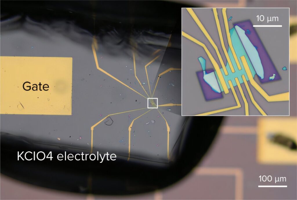
A photograph of the field-effect transistor. The turquoise area in the center of the inset is a flake of molybdenum disulfide, which can be a superconductor, metal, semiconductor or insulator. Credit: Nano Letters (2024). DOI: 10.1021/acs.nanolett.4c04134

A RIKEN study shows that squeezing the right amount of potassium ions between the atomic layers of molybdenum disulfide can turn it from a semiconductor into a metal, superconductor or insulator. The same layered material can be made to behave as a superconductor, metal, semiconductor or insulator by using a transistor device developed by RIKEN physicists to tweak its electronic properties.

The study is published in the journal Nano Letters.

“The variety of electronic properties based on a single material is highly intriguing to us from a materials science perspective,” says Yoshihiro Iwasa of the RIKEN Center for Emergent Matter Science, who led the team.

The material is molybdenum disulfide (MoS2), which can be isolated as an incredibly thin crystal containing layers of molybdenum atoms sandwiched by sulfur atoms. These sulfur atoms can be arranged in different ways, creating two distinct phases known as 2H and 1T. The 2H phase is a semiconductor, whereas the 1T phase is metallic.

“2H molybdenum disulfide is highly promising for use in next-generation semiconductor devices,” notes Iwasa.

The RIKEN researchers have now studied this phase transition in greater detail. They built a device known as a field-effect transistor and connected it to a sample of 2H molybdenum disulfide. By varying the transistor voltage, they could precisely guide potassium ions into the material.

As more potassium entered the material, the material’s phase suddenly changed from 2H to 1T—roughly when there were two potassium ions for every five molybdenum atoms.

Then, by inserting the right amount of potassium and cooling the sample to –268°C, the researchers found that the 1T phase became a superconductor.

See also  Thin coating of MXene material could replace thick layers of insulation

Although superconductivity had previously been seen in the 2H phase, this was unexpected for the 1T phase, and it occurred at a different temperature. “The biggest surprise for us is that we observed superconductivity when we introduced potassium ions,” says Iwasa.

More surprises were in store. The material switched from being a metal to an insulator when the researchers allowed potassium to leak out of 1T molybdenum disulfide until it contained relatively low levels of the ions, and set its temperature at –193°C.

“We found this interesting because we didn’t expect this phenomenon to occur,” says Iwasa.

These results demonstrate that introducing potassium ions in this way is a powerful method for controlling the structure and properties of two-dimensional materials like molybdenum disulfide. The method could help to uncover new superconductors.

“We’ve been developing this method over the past decade,” says Iwasa. “And we’ve shown that it is useful not only for exploring novel properties of superconductors and related electronic phases, but also for discovering new superconductors.”


Source link

electronic Material properties reshapes transistor
Share. Facebook Twitter Pinterest LinkedIn Tumblr Email

Related Posts

A new molecular model of bilayer graphene with higher semiconducting properties

May 31, 2025

5 Nanomaterial Innovations That Didn’t Deliver (Yet)

May 30, 2025

Scientists identify new 2D copper boride material with unique atomic structure

May 30, 2025

Nanoscale biosensor lets scientists monitor molecules in real time

May 30, 2025

How should we govern nanotechnology?

May 29, 2025

The Future of Needle-Free Immunization

May 28, 2025

Comments are closed.

Top Articles
News

Nanoneedle breakthrough gives hope for cheaper cancer treatment

News

Researchers find innovative way to store and process information by maintaining valley polarization at room temperature

News

New quantum material puts eco-friendly methanol conversion in reach

Editors Picks

A new molecular model of bilayer graphene with higher semiconducting properties

May 31, 2025

5 Nanomaterial Innovations That Didn’t Deliver (Yet)

May 30, 2025

Scientists identify new 2D copper boride material with unique atomic structure

May 30, 2025

New contact lenses allow wearers to see in the near-infrared

May 30, 2025
About Us
About Us

Your go-to source for the latest nanotechnology breakthroughs. Explore innovations, applications, and implications shaping the future at the molecular level. Stay informed, embrace the nano-revolution.

We're accepting new partnerships right now.

Facebook X (Twitter) Instagram Pinterest
Our Picks

Lipid nanoparticle-mRNA regimen reverses inflammation and aids recovery from diabetic wounds in mice

May 27, 2024

New opportunities for metasurfaces in optoelectronics

January 1, 2025

Diamond bonding technique could improve both quantum and conventional electronics

October 26, 2024

Subscribe to Updates

Get the latest creative Nano Tech news from Elnano.com

© 2025 Elnano.com - All rights reserved.
  • Contact
  • Privacy Policy
  • Terms & Conditions

Type above and press Enter to search. Press Esc to cancel.

Cleantalk Pixel