Close Menu
  • News
  • Medical
  • Technology
  • Nanomaterials
  • Research
  • Blog
    • Nasiol.com
  • Contact
    • Tech7685@gmail.com
What's Hot

Large-aperture MEMS modulator paves way for high-speed, energy-efficient optical communication systems

May 11, 2025

Dual-stage monitoring technique for nanocomposites can streamline manufacturing and property tracking

May 11, 2025

Probing the molecular mechanisms of metastasis

May 10, 2025
Facebook X (Twitter) Instagram
Nanotech – Nanomaterials | Medical | Research | News Stories Updated Daily Nanotech – Nanomaterials | Medical | Research | News Stories Updated Daily
  • News
  • Medical
  • Technology
  • Nanomaterials
  • Research
  • Blog
    • Nasiol.com
  • Contact
    • Tech7685@gmail.com
Facebook X (Twitter) Instagram
Nanotech – Nanomaterials | Medical | Research | News Stories Updated Daily Nanotech – Nanomaterials | Medical | Research | News Stories Updated Daily
Home»News»Thickness-Dependent Stress in Indium Tin Oxide Thin Films
News

Thickness-Dependent Stress in Indium Tin Oxide Thin Films

January 11, 2024No Comments3 Mins Read
Facebook Twitter Pinterest Telegram LinkedIn Tumblr WhatsApp Email
Thickness-Dependent Stress in Indium Tin Oxide Thin Films
Share
Facebook Twitter LinkedIn Pinterest Telegram Email

Transparent conductive thin films find extensive applications in semiconductor devices, including solar cells, liquid crystal displays, light-emitting diodes, and various sensors. Indium tin oxide (ITO) is widely used as a transparent layer due to its excellent electrical conductivity, optical transparency, and nonlinearity. ITO film deposition by sputtering is favored for its ability to produce films with a compact structure and high transmittance.

During film growth, induced film stresses can affect device fabrication and performance:

  • Stress-induced wafer bow affects device planarity and subsequent production processes;
  • Film stress can alter the physical device properties, potentially compromising reliability.

Experiment Overview

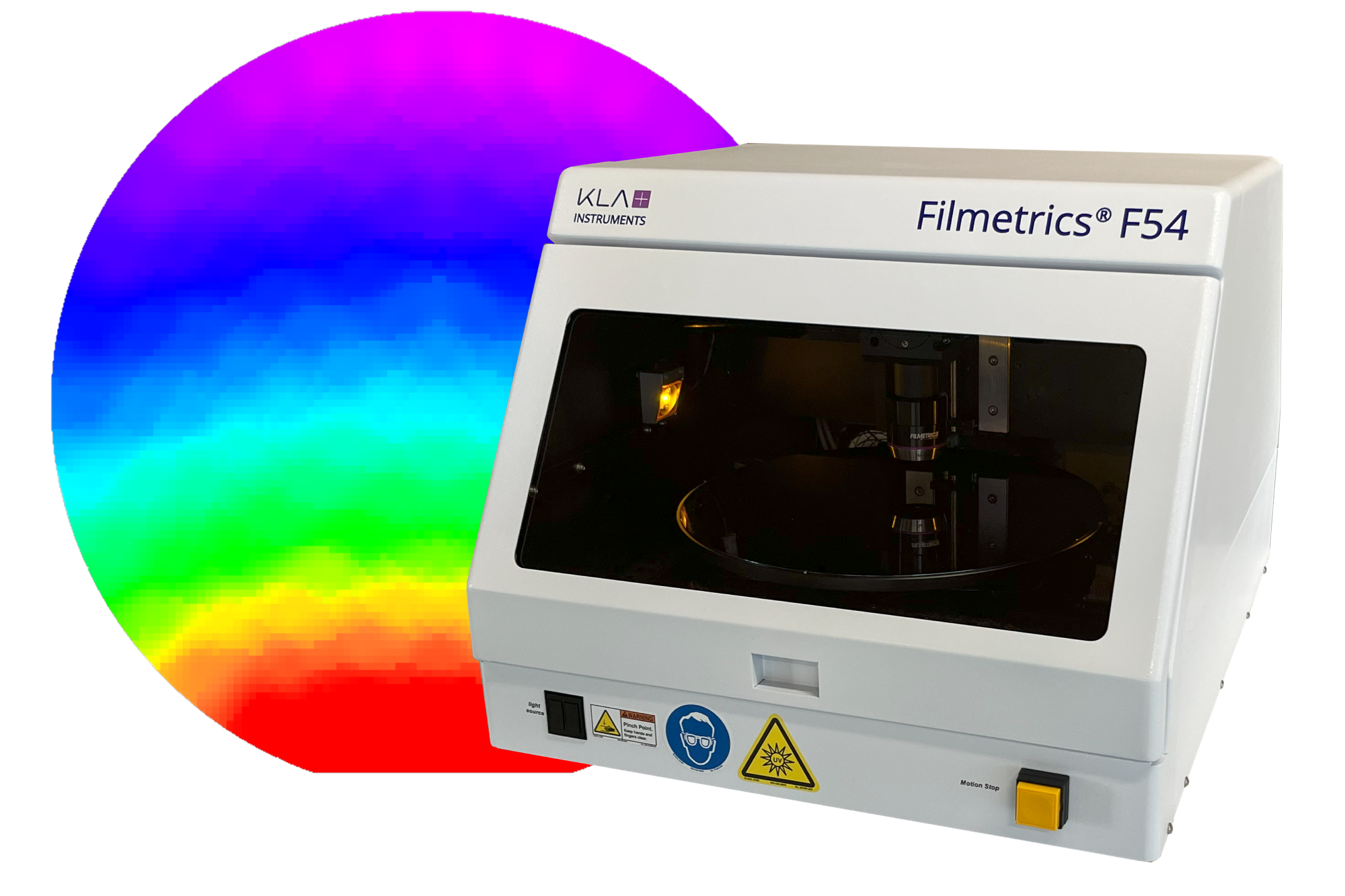
Nine different values of sputtered ITO film thickness were first measured using a Filmetrics® F50-UVX reflectometer from KLA Instruments™. Wafer bow and stress measurements were then performed using the KLA Instruments HRP®-260 automated stylus profiler, as shown in Figure 1. For the wafer bow measurement, the system automatically rotates the sample after each scan to generate a 3-dimensional (3D) bow map from which the software automatically calculates the 3D stress map using the Stoney equation, as shown in Figure 2. Next, the grain structure of the deposited films was evaluated by AFM, as shown in Figures 3 and 4. Finally, the elastic moduli of the ITO films were evaluated by nanoindentation using the Nano Indenter® G200X from KLA Instruments.

Figure 1. (a) 3D bow of ITO (14nm)/glass; (b) 3D bow of ITO (559nm)/glass; (c) 2D bow of ITO/glass with ITO thickness ranging from 14 to 559 nm; (d) Bow as a function of ITO film thickness measured at two distinct time points.

See also  Researchers develop novel 'super-tetragonal' sacrificial layer for freestanding oxide membranes

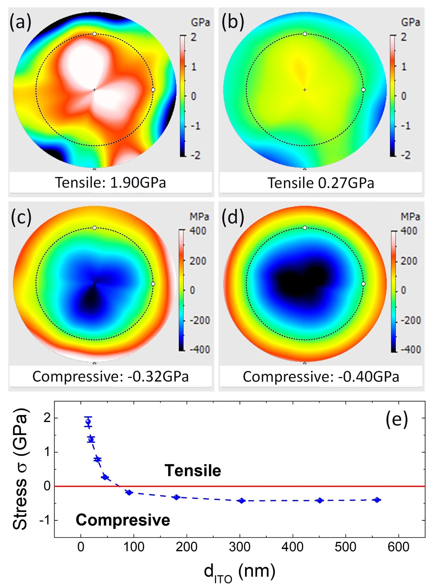
Figure 2. 3D stress of ITO/glass with different ITO thicknesses: (a) dITO = 14 nm; (b) dITO = 45 nm; (c) dITO = 180 nm; (d) dITO = 559 nm. (e) ITO film stress versus film thickness.


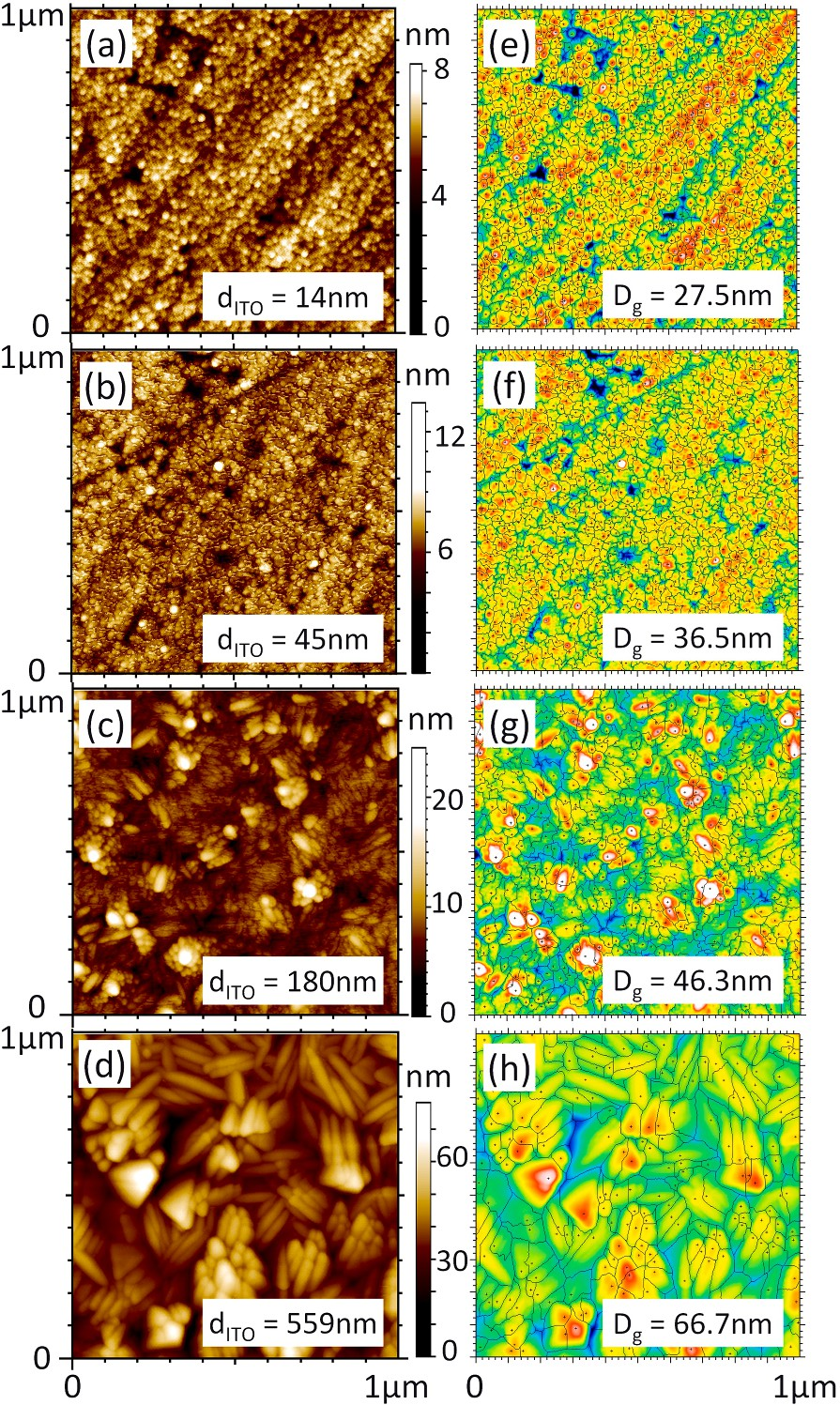
Figure 3. (a)-(d): AFM images of the ITO/glass with different ITO thicknesses; (e)-(h): Grain size analysis with Apex analysis software.

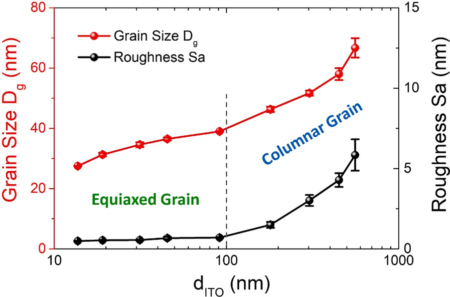
Figure 4. Grain size and surface roughness shown as a function of ITO thickness.

Summary of Results

The investigation revealed a transition of stress type from tensile to compressive as the thickness of the ITO films increased. AFM analysis of the surface morphology of the ITO films indicated a three-dimensional growth mode, with a transformation from equiaxed to columnar grain structure during deposition. Further examination revealed that the tensile stress originated from the impingement and coalescence of newly formed equiaxed grains. As the film thickness increased, fewer equiaxed grains emerged, leading to the dominance of compressive stress. The compressive stress was attributed to the incorporation of excess material in the boundaries of columnar grains.

Further Information

For additional details of the experiment and results, please read the original article as published in Thin Solid Films. For more information on the KLA Instruments metrology systems used in this experiment, please visit the KLA Instruments website:

Visit KLA Instruments at SPIE Photonics West January 30 – February 1, 2024

You are warmly invited to meet KLA’s experts at SPIE Photonics West Booth 1767, January 30 – February 1, 2024, in San Francisco. 

Source link

Films Indium oxide Stress ThicknessDependent thin Tin
Share. Facebook Twitter Pinterest LinkedIn Tumblr Email

Related Posts

Large-aperture MEMS modulator paves way for high-speed, energy-efficient optical communication systems

May 11, 2025

Dual-stage monitoring technique for nanocomposites can streamline manufacturing and property tracking

May 11, 2025

Probing the molecular mechanisms of metastasis

May 10, 2025

AI-powered electronic nose detects diverse scents for health care and environmental applications

May 10, 2025

Microbubble dynamics in boiling water enable precision fluid manipulation

May 9, 2025

Unique molecule may lead to smaller, more efficient computers

May 9, 2025

Comments are closed.

Top Articles

Experiments show coating rice seedling with nanoscale carbon dots from durian helps rice plants thrive in salty soil

News

Generative design tool relies on grammar rules for finding best shape

News

Nanomaterials may enhance plant tolerance to high soil salt levels

Editors Picks

Large-aperture MEMS modulator paves way for high-speed, energy-efficient optical communication systems

May 11, 2025

Dual-stage monitoring technique for nanocomposites can streamline manufacturing and property tracking

May 11, 2025

Probing the molecular mechanisms of metastasis

May 10, 2025

AI-powered electronic nose detects diverse scents for health care and environmental applications

May 10, 2025
About Us
About Us

Your go-to source for the latest nanotechnology breakthroughs. Explore innovations, applications, and implications shaping the future at the molecular level. Stay informed, embrace the nano-revolution.

We're accepting new partnerships right now.

Facebook X (Twitter) Instagram Pinterest
Our Picks

Fluorescent nanomaterial could transform how we visualize fingerprints

September 23, 2024

Researchers develop new nanoparticle to deliver drugs to immune system cells

March 4, 2024

Sensor technology uses nature’s blueprint and machinery to monitor metabolism in body

April 4, 2025

Subscribe to Updates

Get the latest creative Nano Tech news from Elnano.com

© 2025 Elnano.com - All rights reserved.
  • Contact
  • Privacy Policy
  • Terms & Conditions

Type above and press Enter to search. Press Esc to cancel.

Cleantalk Pixel