


The sustained reduction in the size of transistor devices is due, in part, to the replacement of silicon oxide with hafnium oxide as the gate oxide in MOSFETS in the mid-2000s.1
Hafnium oxide (HfO2) serves as a high-k dielectric material and is one of the few binary oxides that remain thermodynamically stable with silicon. It can therefore be naturally incorporated into memory and logic devices. For instance, in 2007, Intel announced the inclusion of hafnium-based high-k metal gates in its processors.2
This innovative transistor design aimed to have lower power consumption and minimized electricity leaks, all while providing enhanced performance through downscaling.
In 2011, a technique for producing ferroelectric hafnium oxide thin films was described.3 All bulk phases of hafnium oxide possess centrosymmetric crystal structures and, as a result, do not show ferroelectricity.
However, when a hafnium oxide thin film is doped with silicon oxide and crystalized under mechanical encapsulation (called “capping”), it generates crystalline phases that are non-centrosymmetric, and thus estimated to be ferroelectric.4
This ferroelectric phase is orthorhombic, a result of mechanical confinement, preventing the tetragonal to monoclinic transformation that would otherwise take place. Ferroelectric hafnium oxide films create opportunities for intriguing devices that leverage silicon/ ferroelectric junctions.
Ferroelectric transistors (FeFETS) hold potential as low-power, ultrafast, and non-volatile memory systems, possibly becoming a competitor to current flash technology.5-7
A problem in assessing hafnium oxide thin films lies in their notably weak piezoelectric response, a characteristic feature of ferroelectric materials. Piezoresponse force microscopy (PFM) is often conducted at the contact resonance frequency to capitalize on the signal’s resonance enhancement.8
The contact resonance frequency, however, shifts as the tip scans various topographic features, introducing crosstalk artifacts that may obscure the piezoelectric response.
Asylum Research’s exclusive Dual Amplitude Resonance Tracking (DART™) mode monitors contact resonance shifts, thereby reducing the impact of topography on the measurement. Figures 1 and 2 show DART PFM images of silicon-doped hafnium oxide thin films, clearly displaying poled piezoelectric domains.
The sample is a 10 nm thin film in its initial state after crystallization, before wake-up cycling. The data was obtained from customer samples using an Asylum Research Cypher S AFM.
Sample courtesy of Thomas Kämpfe at the Fraunhofer Institut, Dresden, Germany
Figure 1. DART PFM amplitude (left) and phase (right) data overlaid on a 3D representation of the surface topography of a 10 nm Si:HfO2 thin film (3 μm scan size). The phase image clearly shows different poled domains. Image Credit: Asylum Research – An Oxford Instruments Company
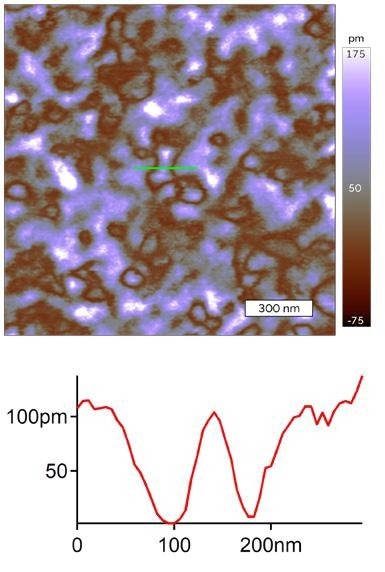
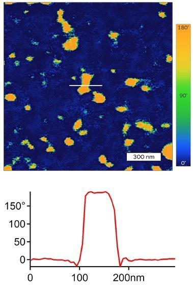
Figure 2. DART PFM amplitude (top) and phase (bottom) images of the same Si:HfO2 thin film. The smaller 1.5 μm scan size makes it simpler to measure individual domains. Here cross-sections were measured across the indicated lines, which indicate that the domains have characteristic dimensions on the order of 100 nm and that the domains are oppositely poled (~180°) relative to the surrounding phase. Image Credit: Asylum Research – An Oxford Instruments Company
References and Further Reading
- Zhu, H., C. Tang, L. R. C. Fonseca, and R. Ramprasad. “Recent progress in ab initio simulations of hafnia-based gate stacks.” Journal of Materials Science 47, no. 21 (2012): 7399-7416.
- Intel News Release: “Intel’s Fundamental Advance in Transistor Design Extends Moore’s Law, Computing Performance: Sixteen Eco-Friendly, Faster and ‘Cooler’ Chips Incorporate 45nm Hafnium-Based High-k Metal Gate Transistors” https://www.Intel.com/pressroom/archive/releases/2007/20071111comp. htm
- Böscke, T. S., J. Müller, D. Bräuhaus, U. Schröder, and U. Böttger. “Ferroelectricity in hafnium oxide thin films.” Applied Physics Letters 99, no. 10 (2011): 102903.
- Polakowski, Patrick, and Johannes Müller. “Ferroelectricity in undoped hafnium oxide.” Applied Physics Letters 106, no. 23 (2015): 232905.
- NamLab (Nanoelectronic Materials Laboratory) Website: “Hafnium Oxide Based Ferroelectric Memory” http://www. namlab.de/research/reconfigurable-devices/hafnium-oxidebased-ferroelectric-memory
- Dünkel, S., M. Trentzsch, R. Richter, P. Moll, C. Fuchs, O. Gehring, M. Majer, et al. “A FeFET based super-low-power ultra-fast embedded NVM technology for 22nm FDSOI and beyond.” In Electron Devices Meeting (IEDM), 2017 IEEE International, pp. 19-7. IEEE, 2017.
- Trentzsch, M., S. Flachowsky, R. Richter, J. Paul, B. Reimer, D. Utess, S. Jansen, et al. “A 28nm HKMG super low power embedded NVM technology based on ferroelectric FETs.” In Electron Devices Meeting (IEDM), 2016 IEEE International, pp. 11-5. IEEE, 2016.
- Rodriguez, Brian J., Clint Callahan, Sergei V. Kalinin, and Roger Proksch. “Dual-frequency resonance-tracking atomic force microscopy.” Nanotechnology 18, no. 47 (2007): 475504.

This information has been sourced, reviewed, and adapted from materials provided by Asylum Research – An Oxford Instruments Company.
For more information on this source, please visit Asylum Research – An Oxford Instruments Company.
