


The high-resolution imaging capability of atomic force microscopy (AFM) can be extended to enable a wide range of characterization methods to study electrical, mechanical, thermal, and other properties of materials and devices. AFM is often used to measure devices during actuation or operation while applying external stimuli, such as specific illuminations, magnetic fields, or electrical drive signals.
When characterizing nanoelectrical structures, such as quantum devices, semiconductor devices, and 1D/2D materials, it may be necessary to measure the response to signals sent to electrical contacts under operating conditions. However, managing the addition of electrical contacts to objects of interest can be a challenge.
Work-intensive methods like metal deposition, wire bonding, or silver paint application are commonly utilized, which can be limiting to certain device geometries or sample types.
Alternatively, microprobers offer a flexible, user-friendly option for AFM experiments that require multiple electrical contacts. This article examines ways to easily implement microprobers on Bruker’s Dimension® AFMs and provides case studies that illustrate the capability and flexibility of this approach.
Instrumentation
Bruker’s Dimension AFMs provide all the required components and features that are essential for combining AFM/microprobing experiments in air as well as in a glovebox (for glovebox-compatible instruments).
The platform is low-noise and low-drift and supports a large sample area that can accommodate multiple microprobers and an extensive array of geometries and sample sizes. Using a scan-by-tip design, Dimension AFMs enable the addition of microprobers and cabling without degrading performance. This is in contrast to scan-by-sample instruments that can be hindered by additional mass or constrained by moving cables.
Bruker also provides the option of an AFM tip holder with high clearance, which provides maximum flexibility for positioning the microprobers close to the tip/sample contact. Lastly, Dimension AFMs have impressive control electronics, with extra channels that can be used to create and apply AC or DC signals to the microprobers. These signals are easy to control with the native AFM software.
Figure 1. A Dimension Icon AFM with three Imina microprobers positioned onto (a) a small sample mounted on an SEM-compatible stub, and (b) a wafer sample with a tip holder optimized for high clearance. Image Credit: Bruker Nano Surfaces and Metrology
Imina Technologies’ probers, already well-proven for similar measurements inside SEMs, meet all requirements set by AFM-level measurements. The miBot™ microprobers offer a compact design with both coarse movement control for centimeter-scale distances and finer nanometer-scale movements for rotation, XY, and tilt.
Adaptation to different samples and experimental setups is easy with flexible installation and compatibility with a range of needles/electronics. These low-drift, low-noise microprobers also offer safe, easy, and rapid probe landing.
Setup and Workflow
In Figure 1a, three Imina probers are positioned onto a small sample (mounted onto an SEM-compatible stub) in a Dimension Icon® AFM. A high-clearance tip holder is also integrated into the AFM.
Special add-ons can also be integrated for specific electrical AFM measurements, including scanning spreading resistance microscopy (SSRM), scanning capacitance microscopy (SCM), conductive AFM (C-AFM) and tunneling AFM (TUNA).
The instrument in Figure 1a, for instance, shows the PeakForce TUNA™ module hardware mounted onto the AFM scanner head. Figure 1b shows a similar setup with a wafer sample.
A common workflow would consist of these steps:
- Load the AFM tip and sample. Complete the usual focus tip, focus surface, and navigate to area of interest steps.
- Using the integrated optical camera as a guide, bring the Imina probers close to the area of interest. Position the probers on the device of interest, making sure to leave enough space to position the AFM tip.
- Follow the usual engage procedure to move the tip to the area of interest, begin scanning, and then complete the fine positioning of the AFM tip.
- Activate the electrical settings and complete the in-situ AFM experiment.
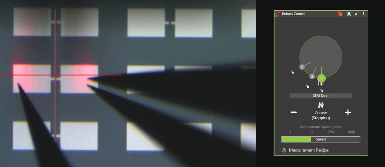
Figure 2. Software view of three Imina microprobers positioned onto the device, prior to engaging the AFM tip onto the sample surface. The Imina Technologies Pricisio™ software is also displayed. Image Credit: Bruker Nano Surfaces and Metrology
Figure 2 shows Step 2 of the above workflow and the optical camera view of three Imina probes that have been positioned on the contact pads of a device. It also shows the Imina probe navigation software.
The microprober needles are easy to position with micrometer resolution, which is limited only by the optical resolution of the integrated camera. The red crosshairs indicate the position where the AFM tip will engage on the sample surface.
Case Studies
For the first case study, potential distribution was mapped on a sample with metal lines on an isolating substrate. The metal lines formed an interlaced network; even lines were electrically connected to each other towards one side of the sample, while odd lines were connected towards the other side of the sample.
Two Imina microprobers were placed on specific lines (one odd and one even), as illustrated in the schematic (Figure 3a) and the optical image (Figure 3b). The DC voltages created by the AFM controller were then applied to the microprobers. The AFM tip then completed a scan across several lines in KPFM mode, and the surface potential distribution was mapped on the device structure.
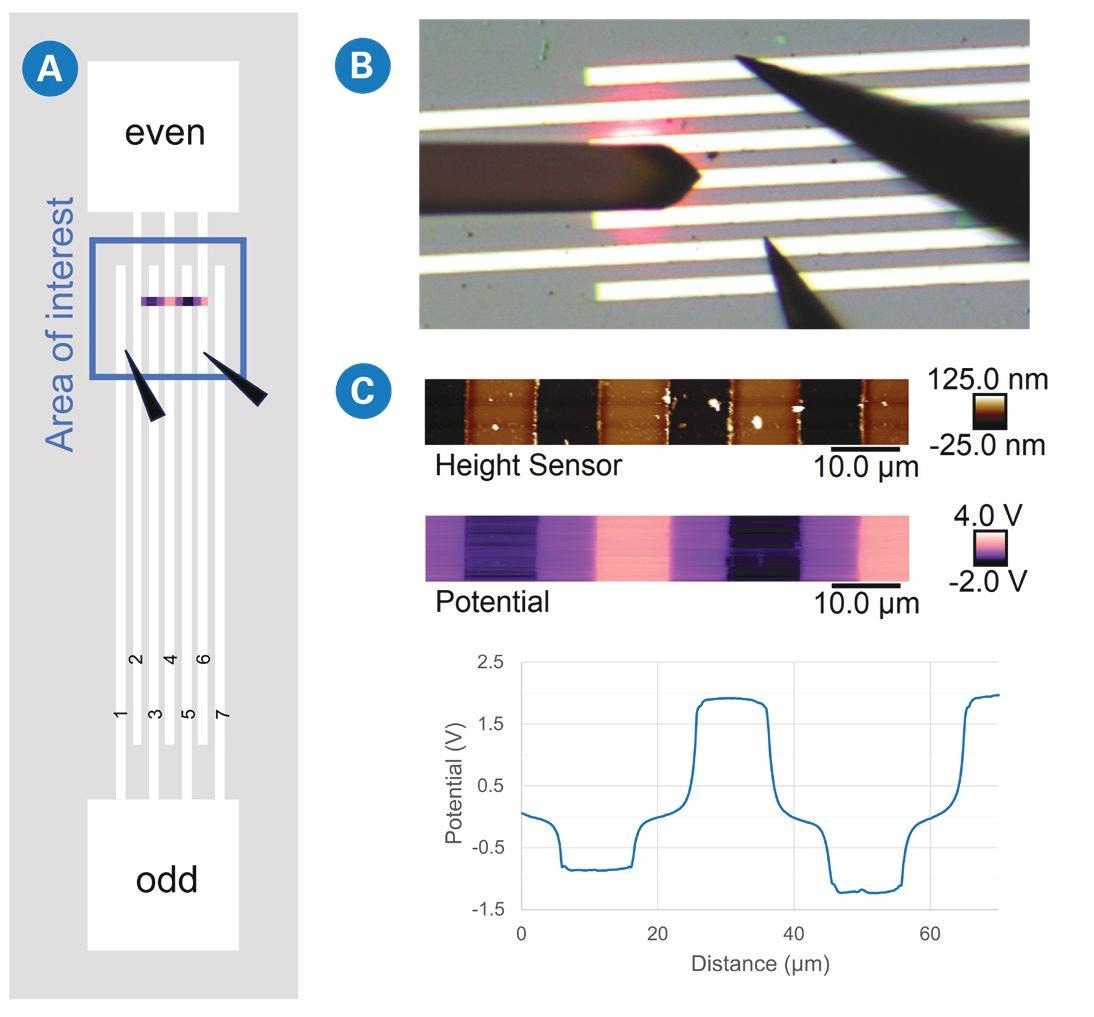
Figure 3. (a) Schematic representation and (b) optical camera image of Imina microprobers positioned onto a structure with interlaced lines. (c) KPFM data collected from the area of interest in (a) while a voltage of -2 V is applied to the odd lines and +2 V to the even lines. The average potential profile is also plotted over the same scan distance. Image Credit: Bruker Nano Surfaces and Metrology
The odd lines received a voltage of -2 V, while the even received +2 V. Figure 3c details the KPFM results across several lines. The averaged potential profile throughout the structure shows that the voltage is close to 2 V at the even lines while it is nearer to -1 V at the odd line. The same potential is not shown at all odd lines.
The potential also shows a gradual change in the isolating areas between individual lines. The potential drops that were observed in the odd lines can be rationalized by a resistance drop in the metal lines—the measurement site is quite far from where the microprober applies the voltage.
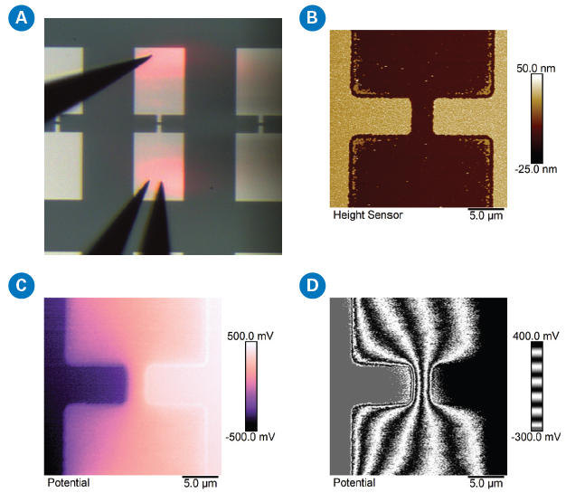
Figure 4. (a) View from the optical camera integrated into the Bruker Dimension Icon AFM showing three Imina microprobers and area of interest on an open-circuit device for KPFM scan. (b) AFM height map of the area of interest marked in (a). (c, d) KPFM potential measurement on the open-circuit device while applying -0.5 V and +0.5 V to the contacts. Image Credit: Bruker Nano Surfaces and Metrology
In the next case study, seen in Figure 4, there are three Imina probers positioned onto two metal pads and connected by a 5 μm wide metal line. Figure 4a shows the optical image, and Figure 4b shows the AFM height image.
KPFM was used to measure the surface potential distribution in the noted area of interest on the device while applying -0.5 V and +0.5 V to the contacts. Figure 4c shows the surface potential color image and demonstrates the voltage available on both contacts. The greyscale contour-line image in Figure 4d delineates the equipotential lines in the dielectric area between the contacts.
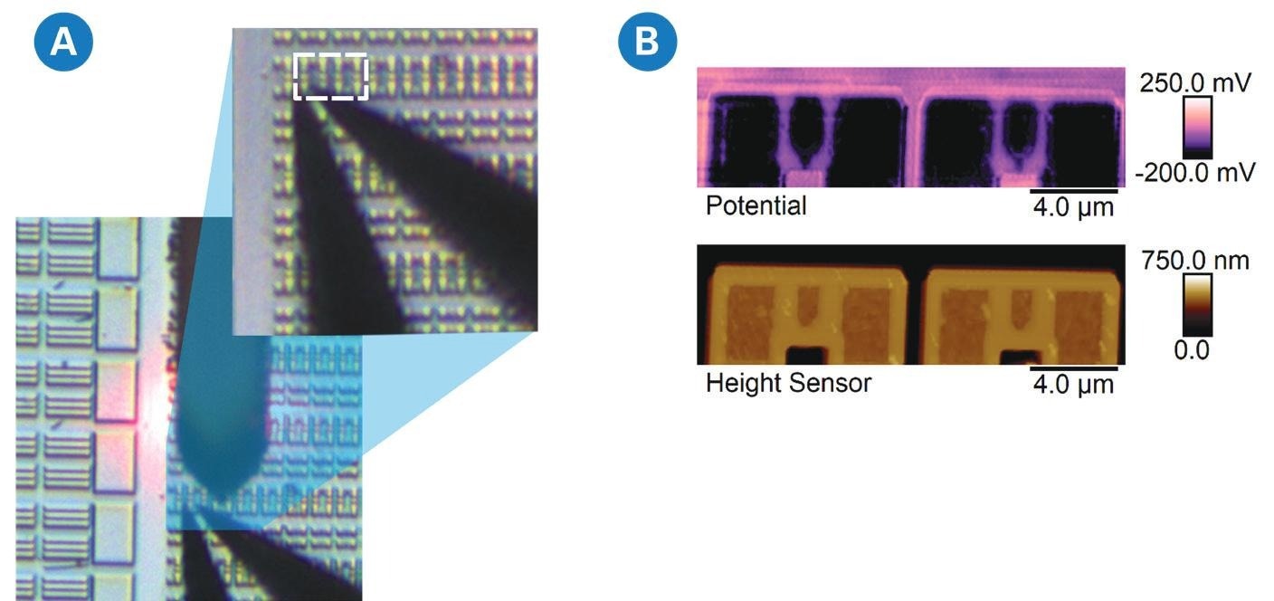
Figure 5. (a) Two Imina microprobers positioned only a few microns apart on the source/drain regions of transistors in an SRAM device, shown with and without (inset) the AFM probe inserted. (b) KPFM data collected in the marked area of interest highlighting source/drain (dark) and channel (lighter) areas. Image Credit: Bruker Nano Surfaces and Metrology
As illustrated by Figure 5a, the positioning of the Imina probers is rather flexible. The Figure details two microprobers positioned directly onto the source/drain regions of a de-processed SRAM sample. There are only a few microns of space between the microprobers.
Figure 5b shows how KPFM was completed on devices immediately adjacent to the positions of the microprobers. The image reveals the source/ drain (dark) and channel (brighter) regions of four transistors in this memory cell.
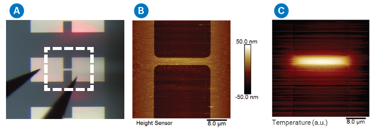
Figure 6. (a) Optical camera image of a short-circuiting device with a marked area of interest for (b) AFM height map and (c) SThM measurement while applying a current through the metal line. Image Credit: Bruker Nano Surfaces and Metrology
This configuration is compatible with a range of advanced characterization modes, including but not limited to magnetic force microscopy (MFM), electric field microscopy (EFM), Kelvin probe force microscopy (KPFM), conductive AFM (C-AFM), piezoresponse force microscopy (PFM), tunneling AFM (TUNA), scanning spreading resistance microscopy (SSRM), scanning capacitance microscopy (SCM), and scanning thermal microscopy (SThM).
To illustrate this, SThM was applied to the device shown in Figure 6, with a short circuit nature. The SThM maps unveil the 2D temperature profile that occurs when a current is passed through the line, with greater temperatures observed at the center of the line (Figure 6c). It is important to note that for SThM, the dedicated SThM tip holder is used, not the high clearance tip holder.
Conclusions
Nanoscale imaging of electrical devices under operation can be facilitated by combining AFM with one or multiple compact microprobers within a few microns from the AFM tip/sample contact. Bruker’s Dimension AFMs are ideal for this type of integration, as they are able to maintain their performance level and wide range of operating modes when adding microprobers.

This information has been sourced, reviewed and adapted from materials provided by Bruker Nano Surfaces and Metrology
For more information on this source, please visit Bruker Nano Surfaces and Metrology
