An international research team led by NYU Tandon School of Engineering and KAIST (Korea Advanced Institute of Science and Technology) has pioneered a new technique to identify and characterize atomic-scale defects in hexagonal boron nitride (hBN), a two-dimensional (2D) material often dubbed “white graphene” for its remarkable properties.
This advance could accelerate the development of next-generation electronics and quantum technologies.
The team reported that it was able to detect the presence of individual carbon atoms replacing boron atoms in hBN crystals. This discovery was made possible by listening to the electronic “noise” in specially designed transistors, akin to hearing a whisper in a quiet room.
The research is published in the journal ACS Nano, which selected the research paper as its cover story for the October 22, 2024 edition.
“In this project, we essentially created a stethoscope for 2D materials,” said Davood Shahrjerdi, one of the paper’s corresponding authors, along with Yong-Hoon Kim. “By analyzing the tiny and rhythmic fluctuations in electrical current, we can ‘perceive’ the behavior of single atomic defects.”
Shahrjerdi is an associate professor in NYU Tandon’s Electrical and Computer Engineering Department, a faculty member of NYU WIRELESS, and the Director of the NYU Nanofabrication Cleanroom (NanoFab) that opened in 2023. Kim is Professor of Electrical Engineering at KAIST. Shahrjerdi and Kim are also affiliated faculty at NYU-KAIST Global Innovation and Research Institute, where they lead collaborations in the NYU-KAIST Next-Gen Semiconductor Devices and Chips research group.
The NYU-KAIST partnership was officially launched at NYU in September 2022 by the President of South Korea. This historic partnership combines the distinctive strengths of both universities to drive advances in research and education and currently involves over 200 faculty from both institutions.
Single-crystal hBN has emerged as a wonder material in scientific circles, promising to transform fields from unconventional electronics to quantum technologies.
hBN’s atomically thin structure and excellent insulating properties make it an ideal medium for hosting exotic physical phenomena that are not possible with conventional materials. The atomic defects in hBN can degrade its electronic properties, sometimes in ways that could be harnessed for quantum technologies.
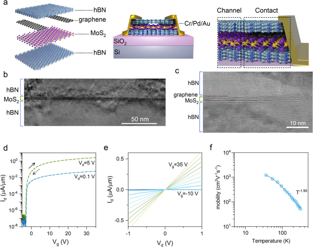
The NYU team built a transistor using a few-layer thin molybdenum disulfide (another 2D semiconducting material) sandwiched between layers of hBN. By cooling this device to cryogenic temperatures and applying precise electrical voltages, they were able to observe discrete jumps in the current flowing through the transistor.
These jumps, known as random telegraph signals (RTS), occur when electrons are captured and released by defects in the hBN. By carefully analyzing these signals at different temperatures and voltages, the team was able to determine the energy levels and spatial locations of the defects.
“It’s like we’ve developed a microscope that can ‘see’ individual atoms, but instead of light, we’re using electricity,” said Zhujun Huang, the paper’s first author who was an NYU Tandon ECE Ph.D. student at the time of the study.
The KAIST team then used advanced computer simulations to clarify the atomistic origins of the experimental observations. Specifically, this combination of experiment and theory revealed that the defects are carbon atoms sitting in places where boron atoms should be in the hBN crystal structure.
“Understanding and controlling the defects in 2D materials could have significant implications for the future of electronics and quantum technologies,” explained Sharhrjerdi and Kim. “For example, we might be able to create more perfect quantum material platforms for discovery of new physics or single-photon emitters for secure communications.”
This work adds to NYU Tandon’s expanding portfolio in quantum materials and device technologies, aligning with the CHIPS and Science Act’s semiconductor innovation goals. Prior research demonstrated nanomanufacturing principles for low-disorder quantum materials and their potential in devices when integrated with superconductors.


