Close Menu
  • News
  • Medical
  • Technology
  • Nanomaterials
  • Research
  • Blog
    • Nasiol.com
  • Contact
    • Tech7685@gmail.com
What's Hot

Large-aperture MEMS modulator paves way for high-speed, energy-efficient optical communication systems

May 11, 2025

Dual-stage monitoring technique for nanocomposites can streamline manufacturing and property tracking

May 11, 2025

Probing the molecular mechanisms of metastasis

May 10, 2025
Facebook X (Twitter) Instagram
Nanotech – Nanomaterials | Medical | Research | News Stories Updated Daily Nanotech – Nanomaterials | Medical | Research | News Stories Updated Daily
  • News
  • Medical
  • Technology
  • Nanomaterials
  • Research
  • Blog
    • Nasiol.com
  • Contact
    • Tech7685@gmail.com
Facebook X (Twitter) Instagram
Nanotech – Nanomaterials | Medical | Research | News Stories Updated Daily Nanotech – Nanomaterials | Medical | Research | News Stories Updated Daily
Home»News»Scientists discover ‘flipping’ layers in heterostructures cause changes in their properties
News

Scientists discover ‘flipping’ layers in heterostructures cause changes in their properties

October 21, 2023No Comments4 Mins Read
Facebook Twitter Pinterest Telegram LinkedIn Tumblr WhatsApp Email
Scientists discover ‘flipping’ layers in heterostructures cause changes in their properties
Share
Facebook Twitter LinkedIn Pinterest Telegram Email
Two different vdW heterostructures. The left consists of WS2 on top of WSe2, and the right consists of WSe2 on top of WS2. The two TMD layers are stacked on top of h-BN and Si/SiO2, which are substrates. Credit: Institute for Basic Science

Transition metal dichalcogenide (TMD) semiconductors are special materials that have long fascinated researchers with their unique properties. For one, they are flat, one-atom-thick two-dimensional (2D) materials similar to that of graphene. They are compounds that contain different combinations of the transition metal group (e.g., molybdenum, tungsten) and chalcogen elements (e.g., sulfur, selenium, tellurium).

What’s even more fascinating is that assembling different TMD layers into vertical stacks creates a new artificial material called a van der Waals (vdW) heterostructure. By incorporating different materials, it becomes possible to combine the properties of individual layers, producing new optoelectronic devices with tailor-made properties. This opens the door to exploring fundamental physics, such as interlayer excitons, twistronics, and more.

However, until now, no scientists have studied whether changing the stacking order affects the spectroscopic properties of these heterostructures. For a long time, the lack of understanding of TMD heterostructures led to a questionable hypothesis that altering the stacking order of the layers does not affect their properties. The study is published in the journal Nature Communications.

This was recently debunked by a team of researchers at the Center for Integrated Nanostructure Physics (CINAP), Institute for Basic Science (IBS) in South Korea. Led by Professor LEE Young Hee the group discovered that the sequential order of the layers in heterostructures affects the generation of “dark excitons” within the material. This finding suggested the added importance of considering stacking sequential order dependence of these materials for further use in real device applications.

Excitons represent an electron and a positively charged hole (a location where an electron is absent) bound together by electrostatic attraction in a solid material, typically a semiconductor crystal. Monolayer TMD semiconductors have a direct bandgap and exhibit optically accessible “bright excitons.” At the same time, there are also “dark excitons,” that are challenging to study due to their invisibility. However, the underlying mechanisms that give rise to these anomalies are not fully understood.

See also  Researchers discover way to reverse brain aging caused by COVID-19

The IBS researchers observed a remarkable phenomenon: the emergence or disappearance of additional photoluminescence (PL) peaks based on different stacking sequences. This previously unreported effect has been confirmed to be reproducible across multiple heterostructures.

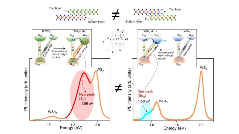
The researchers attributed the origin of these additional peaks to the emergence of dark exciton exclusively located in the top layer of the heterostructure, which is further confirmed by scanning tunneling microscopy (STM). Researchers expect that this property can be utilized for optical power switches in solar panels.
Scientists discover 'flipping' layers in heterostructures to cause changes in their properties
Stacking sequence-dependent dark exciton modulation. Left, schematic of WS2 (top)/WSe2 (bottom) hetero-bilayer and their corresponding core-spong PL. A new excitonic feature (red color peak) emerges at the hetero-bilayer region due to the downshifting of the Q-band (inset) only at the heterostructure. Right, opposite stacking of WSe2 (top)/WS2 (bottom) hetero-bilayer and their corresponding PL. The previous dark-exciton peak (red color peak) completely vanished, whereas another new excitonic feature (cyan color peak) emerged at the hetero-bilayer region due to the downshifting of the Q-band (inset) at the heterostructure. Credit: Institute for Basic Science

Dr. Riya Sebait, the first author of the study said, “Our experimental results clearly demonstrate stacking sequence-dependent anomalous properties, which could potentially pioneer a new field of study named ‘fliptronics.’ As we flip or invert the heterostructure, bands undergo a unique renormalization.”

A clean, residue-free interface is necessary to investigate stacking sequential dependent properties. This study represents a significant breakthrough as this was the first time. It was demonstrated that altering the stacking sequential order in the heterostructure can lead to changes in its physical properties.

Researchers attempted to explain this flip-induced phenomenon by looking into the microscopic many-particle model, which suggests that layer-dependent strain could be one possible solution to this puzzle.

Assuming that the top layer becomes more strained compared to the bottom layer, the calculated data using the theoretical model shows good agreement with the experimental results. This suggests that this stacking sequence-dependent requires further study, not only for understanding the underlying physics but also for its real-device applications.

Furthermore, this study also facilitates the utilization of momentum-forbidden dark excitons, as due to the unique band renormalization at the heterostructure, it is possible to convert them into bright excitons.

See also  New method to measure entropy production on the nanoscale

Prof. Young Hee Lee, the main-corresponding author said, “This exceptional phenomenon of the emergence of dark excitons at the bilayer heterostructure will inspire other researchers to delve deeper into understanding and harnessing these extraordinary properties towards applications.”

This work was conducted in interdisciplinary collaborations with Prof. Ermin Malic at Philipps-Universität Marburg, Germany, and research fellow Seok Jun Yun from Oak Ridge Laboratory, U.S..

Provided by
Institute for Basic Science


Source link

discover flipping heterostructures layers properties Scientists
Share. Facebook Twitter Pinterest LinkedIn Tumblr Email

Related Posts

Large-aperture MEMS modulator paves way for high-speed, energy-efficient optical communication systems

May 11, 2025

Dual-stage monitoring technique for nanocomposites can streamline manufacturing and property tracking

May 11, 2025

Probing the molecular mechanisms of metastasis

May 10, 2025

AI-powered electronic nose detects diverse scents for health care and environmental applications

May 10, 2025

Microbubble dynamics in boiling water enable precision fluid manipulation

May 9, 2025

Unique molecule may lead to smaller, more efficient computers

May 9, 2025

Comments are closed.

Top Articles

Study reveals surprisingly simple method for determining exchange energy in 2D materials

News

Advances in nanoscale force measurement opens doors to unprecedented biological insights

News

Durable, inexpensive electrocatalyst generates clean hydrogen and oxygen from water

Editors Picks

Large-aperture MEMS modulator paves way for high-speed, energy-efficient optical communication systems

May 11, 2025

Dual-stage monitoring technique for nanocomposites can streamline manufacturing and property tracking

May 11, 2025

Probing the molecular mechanisms of metastasis

May 10, 2025

AI-powered electronic nose detects diverse scents for health care and environmental applications

May 10, 2025
About Us
About Us

Your go-to source for the latest nanotechnology breakthroughs. Explore innovations, applications, and implications shaping the future at the molecular level. Stay informed, embrace the nano-revolution.

We're accepting new partnerships right now.

Facebook X (Twitter) Instagram Pinterest
Our Picks

How Governments are Fueling Nanotech Innovations

November 23, 2023

Digital twin confirms nanotubes can detect cracks in aircraft wing mid-flight

November 23, 2024

Nanoscale Innovation: Transforming Industries and Creating a More Sustainable Future

October 16, 2023

Subscribe to Updates

Get the latest creative Nano Tech news from Elnano.com

© 2025 Elnano.com - All rights reserved.
  • Contact
  • Privacy Policy
  • Terms & Conditions

Type above and press Enter to search. Press Esc to cancel.

Cleantalk Pixel