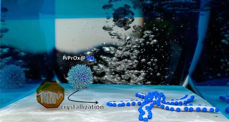
Scientists from the Friedrich Schiller University Jena and the Friedrich Alexander University Erlangen-Nuremberg, both Germany, have successfully developed nanomaterials using a so-called bottom-up approach. As reported in the journal ACS Nano, they exploit the fact that crystals often grow in a specific direction during crystallization. These resulting nanostructures could be used in various technological applications.
“Our structures could be described as worm-like rods with decorations,” explains Prof. Felix Schacher. “Embedded in these rods are spherical nanoparticles; in our case, this was silica. However, instead of silica, conductive nanoparticles or semiconductors could also be used—or even mixtures, which can be selectively distributed in the nanocrystals using our method,” he adds. Accordingly, the range of possible applications in science and technology is broad, spanning from information processing to catalysis.
Understanding and controlling the formation process
“The primary focus of this work was to understand the preparation method as such,” explains the chemist. To produce nanostructures, he elaborates, there are two different approaches: larger particles are ground down to nanometer size, or the structures are built up from smaller components.
“We wanted to understand and control this building-up process,” Schacher describes. For this, the team used individual silicon dioxide particles, known as silica, and grafted chain-like polymer molecules as a sort of shell.
“One could imagine it like hairs on a sphere,” the scientist explains. He adds, “These hairs are made of a material called ‘poly-(isopropyl-oxazoline).’ This substance crystallizes when heated. And that’s the idea of our method: crystals almost never grow in all directions simultaneously but prefer a particular direction. This is known as anisotropy. Thus, we were able to grow our nanostructures deliberately.”
During this process, the team discovered an intriguing phenomenon. “For the polymer to crystallize, it requires tiny amounts that are not bound to a particle surface but are freely present in the reaction solution, acting as a sort of glue. We found out that the required amounts are so small that they are barely detectable. But they are needed,” he adds.
Schacher is particularly excited about the unique collaboration that made this research possible. “Without the excellent cooperation with Prof. Michael Engel from the University of Erlangen, this work would not have been accomplished,” emphasizes the scientist from Jena.
“With the help of computer simulations that depicted behavior across multiple scales, we were able to intricately resolve the complex molecular processes underlying the formation of the nanostructures. This was an exciting challenge,” Engel adds.
Both scientists conclude, “We had the opportunity to participate together in a program of the Kavli Institute for Theoretical Physics (KITP) at the University of California in Santa Barbara earlier this year. During this workshop, we jointly wrote this manuscript. The underlying experiments had of course been conducted beforehand—partially within the framework of the collaborative research center TRR 234 ‘CataLight’ funded by the German Research Foundation. But the inspiring atmosphere of the workshop gave us the necessary momentum to complete the work.”
Provided by
Friedrich-Schiller-Universität Jena


