In recent years, the exceptional structure and fascinating electrical and optical properties of two-dimensional (2D) layered crystals have attracted widespread attention. Examples of such crystals include graphene, black phosphorus (BP), and transition metal dichalcogenides (TMDs).
With their atomic thickness, high carrier mobility, and tunable bandgaps, these materials hold immense promise in various applications and continue to garner significant interest in the scientific community. Graphene, a crystalline structure of tightly packed carbon atoms connected by sp2 hybridization forming a single-layer two-dimensional honeycomb lattice, boasts an electron mobility as high as 2×105 cm2·V−1·s−1.
However, graphene’s short-lived photo-generated carriers attributed to its zero bandgap and extremely low light absorption (2.3%) hinder its device applications. Transition metal dichalcogenides feature wide bandgaps and relatively lower carrier mobility (<200 cm2·V−1·s−1), making them unsuitable for applications in the field of optoelectronic detection.
Due to its unique characteristics, black phosphorus emerges as a highly promising material for infrared detectors. Notably, it exhibits a direct bandgap ranging from 0.34 eV in bulk to 2.1 eV in monolayer form. Furthermore, based on previous studies, black phosphorus possesses a high carrier mobility of approximately 1,000 cm2·V−1·s−1 and a large on/off ratio of 105. These attributes further enhance the potential of black phosphorus as the preferred material for infrared detection applications.
Unfortunately, black phosphorus suffers from poor stability and degrades rapidly in the atmosphere at room temperature, limiting its practical applications. Black arsenic (B-As), as a homolog of phosphorus, shares a similar crystal structure with BP and is expected to exhibit excellent electrical and optical performance, with anticipated high carrier mobility (up to 103 cm2·V−1·s−1).
As previous research has indicated, the bandgap of B-As is highly dependent on the material thickness. Specifically, the indirect bandgap of single-layer B-As ranges from approximately 1-1.5 eV, while bulk B-As is a direct bandgap semiconductor with a bandgap of approximately 0.3 eV.
These findings underscore the importance of considering layer thickness in studying the electronic and optical properties of B-As, demonstrating the potential of this material in various applications.
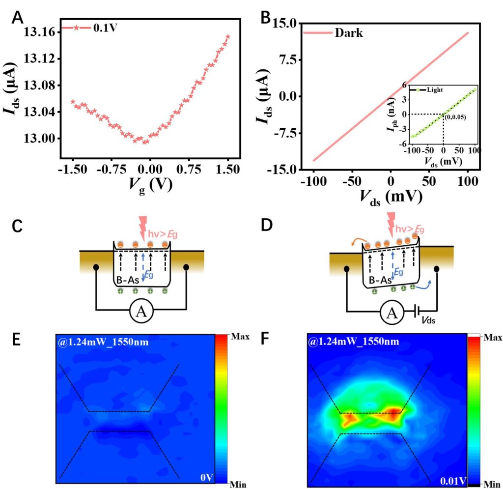
Now, a research group has designed a dual-band photodetector based on black phosphorus for visible and infrared wavelengths. At room temperature, the team discovered through the device’s transfer characteristics and voltage-current characteristics that the prepared device is an n-type depletion-mode FET and exhibits good Ohmic contact.
The research is published in the journal Advanced Devices & Instrumentation.
When the energy of incident laser photons is greater than the bandgap of several layers of B-As (hv > Eg), photo-excited electron-hole pairs can be generated. When the B-As device is in bias mode, the applied electric field effectively separates the photo-generated electron-hole pairs at the interface and injects them into the electrode, thereby generating a photocurrent. The team’s research results indicate that the photoconductive effect is the main light response mechanism of the B-As device in the visible light and infrared bands.
During the experiment, they found a weak signal at zero bias voltage, which they analyzed to be due to the uneven illumination of the laser spot on the channel introducing photothermal current. This may also be attributed to the Dember effect caused by the different diffusion coefficients of electrons and holes, leading to the built-in electric field.
Researchers provided the most intuitive and effective way to display the region where photocurrent is generated through scanning photocurrent maps, used to validate their explanation. A weak photocurrent signal is emitted from the device at 0 V bias, confirming their previous explanation. Increasing the bias voltage by 0.01V at the same position of the channel reveals a significant expansion of the photosensitive area.
This study has successfully developed a B-As photodetector capable of rapid response at room temperature, demonstrating exceptional dual-band light response characteristics. The detector exhibited a peak photoresponsivity of 387.3 mA·W−1 at a near-infrared wavelength of 825 nm without the need for an external bias, and achieved a high detectivity of 1.37×10⁸ Jones.
The response mechanism across the visible to infrared spectrum is primarily attributed to the photoconductive effect. These results not only confirm the superior photoelectric performance of B-As as a narrow-bandgap semiconductor but also showcase its performance comparable to that of black phosphorus (BP), indicating significant potential for application in high-speed optoelectronic devices. Most importantly, the dual-band detection capabilities demonstrated in this research lay a solid foundation for the future development of room-temperature, broadband photodetection technologies.
Provided by
Advanced Devices & Instrumentation


