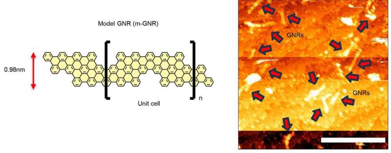
Researchers have developed a method of “wiring up” graphene nanoribbons (GNRs), a class of one-dimensional materials that are of interest in the scaling of microelectronic devices. Using a direct-write scanning tunneling microscopy (STM) based process, the nanometer-scale metal contacts were fabricated on individual GNRs and could control the electronic character of the GNRs.
The researchers say that this is the first demonstration of making metal contacts to specific GNRs with certainty and that those contacts induce device functionality needed for transistor function.
The results of this research, led by electrical and computer engineering (ECE) professor Joseph Lyding, along with ECE graduate student Pin-Chiao Huang and materials science and engineering graduate student Hongye Sun, were recently published in the journal ACS Nano.
“Graphene has been around for a while and it’s been thought of as something that could potentially be a high-speed electronic material, perhaps even a replacement for silicon,” explains Lyding. “But the problem with graphene itself is that it is not a semiconductor.”
Graphene is a one-atom-thick layer of carbon atoms and while it may be the thinnest known material, it is also incredibly strong. Semiconductor properties can be induced in graphene by making it very small or by fabricating it into specific shapes—like ribbons. For this project, atomically-precise GNRs were synthesized by co-author Alexander Sinitskii and his group at the University of Nebraska.
The process of making a transistor out of the GNRs includes putting them on a silicon substrate, connecting wires and running current through the wires to measure the transistor properties. The team has made the critical step of taking the GNRs, that are narrower in diameter than a DNA molecule, and wiring them up. They have developed a technique where the wires are also just a few nanometers wide.
Other researchers have worked on this problem by putting many GNRs on a silicon surface and putting down giant electrodes and hoping for the best. This method, however, introduces a lot of uncertainty. Lyding and his students used a more precise method for wiring up the GNRs. They used a scanning tunneling microscope (an atomic resolution imaging tool) to scan the surface looking for a GNR to use.
In STM, a sharp tip is brought close to a surface—on the order of a nanometer—and scanned across the surface. There is a current flow between the tip and the surface, and when the tip comes across atoms on the surface, like driving over a speedbump, that current flow becomes modulated. This allows for the detection and imaging of the GNRs.
Once they find a GNR, they use the electron beam in the STM to trigger metal deposition from hafnium diboride precursor molecules to create the wires. Co-author Gregory Girolami and his group in the UIUC Chemistry Department synthesized the precursor for this process, called STM direct-write. “Our wiring method is very precise. When we see a GNR, we can just define a pattern that we want, and then we’ll connect it. It’s not just blindly throwing electrodes on the surface,” says Huang.
Another advantage of this method is that it is done in ultra-high vacuum (UHV). This ensures that the material stays clean from atmospheric water and other “junk” that degrades device performance.
The researchers also investigated the electronic character of the GNRs and found that it was changed by putting the metal contacts on. Semiconductor “doping” is the intentional introduction of impurities to change its electronic properties.
Sun explains, “One way to dope GNRs is to use different chemical reactions to change the GNR properties. But that process is hard. The way we do it is by depositing metal. And we can actually choose the kind of metal that we want to put on the GNRs which could also tune the GNR characteristics. That’s one way to essentially dope our GNRs, without actually using dopants.”
Lyding says, “The next step, which we’re working on now, is to make a real transistor and actually measure the transistor characteristics. But we know that we can do this pristine process, using ultra-high vacuum, of making the electrodes that are absolutely necessary for device function.”


