Close Menu
  • News
  • Medical
  • Technology
  • Nanomaterials
  • Research
  • Blog
    • Nasiol.com
  • Contact
    • Tech7685@gmail.com
What's Hot

Rapid nanoparticle simulations could boost efforts to combat air pollution

June 1, 2025

New tool reveals how DNA nanostructures interact with cell membranes

June 1, 2025

New insights show universal applicability of carbyne as a sensor

May 31, 2025
Facebook X (Twitter) Instagram
Nanotech – Nanomaterials | Medical | Research | News Stories Updated Daily Nanotech – Nanomaterials | Medical | Research | News Stories Updated Daily
  • News
  • Medical
  • Technology
  • Nanomaterials
  • Research
  • Blog
    • Nasiol.com
  • Contact
    • Tech7685@gmail.com
Facebook X (Twitter) Instagram
Nanotech – Nanomaterials | Medical | Research | News Stories Updated Daily Nanotech – Nanomaterials | Medical | Research | News Stories Updated Daily
Home»News»Researchers hack a 3D printer to speed up fabrication of bioelectronics
News

Researchers hack a 3D printer to speed up fabrication of bioelectronics

March 5, 2024No Comments2 Mins Read
Facebook Twitter Pinterest Telegram LinkedIn Tumblr WhatsApp Email
Share
Facebook Twitter LinkedIn Pinterest Telegram Email
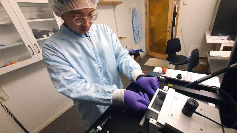
Researchers hacked a 3D printer to speed up fabrication of bioelectronics
Ph.D. student Lee-Lun Lai loads a tray into a 3D microprinter to demonstrate how polymer transistors can be made faster, cheaper and more sustainably. Credit: David Callahan-KTH Royal Institute of Technology

The speed of innovation in bioelectronics and critical sensors gets a new boost with the unveiling of a simple, time-saving technique for the fast prototyping of devices.

A research team at KTH Royal Institute of Technology and Stockholm University reported a simple way to fabricate electrochemical transistors using a standard Nanoscribe 3D micro printer. Without cleanroom environments, solvents, or chemicals, the researchers demonstrated that 3D micro printers could be hacked to laser print and micropattern semiconducting, conducting, and insulating polymers.

Anna Herland, professor in Micro- and Nanosystems at KTH, says the printing of these polymers is a key step in prototyping new kinds of electrochemical transistors for medical implants, wearable electronics and biosensors.

The technique could replace time-consuming processes that require an expensive cleanroom environment. Nor would it involve solvents and developer baths that have a negative environmental impact, says the study’s co-author Erica Zeglio, a faculty researcher with Digital Futures, a research center jointly operated by KTH Royal Institute of Technology and Stockholm University.

“Current methods rely on expensive and unsustainable cleanroom practices,” Zeglio says. “The method we proposed here doesn’t.”

Polymers are core components of many bioelectronic and flexible electronic devices. The applications are diverse, including monitoring living tissues and cells and diagnosing diseases in point-of-care testing.

“Fast prototyping of these devices is time-consuming and costly,” Herland says. “It hinders the widespread adoption of bioelectronic technologies.”

Using ultrafast laser pulses, the new method creates possibilities for the rapid prototyping and scaling of microscale devices for bioelectronics, says co-author and KTH Professor Frank Niklaus. The method could also be used for the patterning of other soft electronic devices, he says. The team applied the new method to fabricate complementary inverters and enzymatic glucose sensors.

See also  Using Einstein's tea leaf paradox to study nanofluids

Herland says the method could advance research in bioelectronic devices and significantly shorten the time-to-market.

“This also creates the possibility of replacing some of the current components with cheaper and more sustainable alternatives,” she says.

The researchers published their results in the journal Advanced Science.

Provided by
KTH Royal Institute of Technology


Source link

Share. Facebook Twitter Pinterest LinkedIn Tumblr Email

Related Posts

Rapid nanoparticle simulations could boost efforts to combat air pollution

June 1, 2025

New tool reveals how DNA nanostructures interact with cell membranes

June 1, 2025

New insights show universal applicability of carbyne as a sensor

May 31, 2025

A new molecular model of bilayer graphene with higher semiconducting properties

May 31, 2025

5 Nanomaterial Innovations That Didn’t Deliver (Yet)

May 30, 2025

Scientists identify new 2D copper boride material with unique atomic structure

May 30, 2025

Comments are closed.

Top Articles
News

Nanomembranes in Pharma: Efficient Separation Solutions

News

Precise stirring conditions key to optimizing nanostructure synthesis

Medical

New nano-thin superbug-slaying material could revolutionize wound healing

Editors Picks

Rapid nanoparticle simulations could boost efforts to combat air pollution

June 1, 2025

New tool reveals how DNA nanostructures interact with cell membranes

June 1, 2025

New insights show universal applicability of carbyne as a sensor

May 31, 2025

A new molecular model of bilayer graphene with higher semiconducting properties

May 31, 2025
About Us
About Us

Your go-to source for the latest nanotechnology breakthroughs. Explore innovations, applications, and implications shaping the future at the molecular level. Stay informed, embrace the nano-revolution.

We're accepting new partnerships right now.

Facebook X (Twitter) Instagram Pinterest
Our Picks

Data Analytics in the Semiconductor Manufacturing Chain

November 22, 2023

The Role of Nanotechnology in Endometriosis Treatment

June 19, 2024

Researchers use multi-phase composition and electrospinning to fabricate SiOC nanofibers

October 29, 2024

Subscribe to Updates

Get the latest creative Nano Tech news from Elnano.com

© 2025 Elnano.com - All rights reserved.
  • Contact
  • Privacy Policy
  • Terms & Conditions

Type above and press Enter to search. Press Esc to cancel.

Cleantalk Pixel