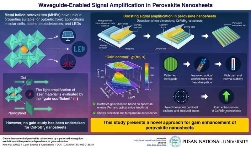
Perovskite materials are still attracting a lot of interest in solar cell applications. Now, the nanostructures of perovskite materials are being considered as a new laser medium. Over the years, light amplification in perovskite quantum dots has been reported, but most of the works present inadequate quantitative analysis.
To assess the light amplification ability, a “gain coefficient” is necessary, whereby the essential characteristic of a laser medium is revealed. An efficient laser medium is one that has a large gain, and scientists have been exploring ways to boost this gain.
Now, in a recent study, a team of researchers led by Professor Kwangseuk Kyhm from the Department of Optics & Mechatronics at Pusan National University in Korea has managed to enhance signal amplification in perovskite nanosheets of CsPbBr3 with a unique waveguide pattern.
Their study is published in the journal Light: Science & Applications.
Perovskite nanosheets are two-dimensional structures arranged in sheet-like configurations on the nanoscale and possess characteristics that make them valuable for various applications.
Their achievement overcomes the shortcomings of CsPbBr3 quantum dots, whose gain is inherently limited due to the Auger process, which essentially shortens the decay time for population inversion (a state in which more members of the system are in higher, excited states than in lower, unexcited energy states).
Prof. Kyhm explains, “Perovskite nanosheets can be a new laser medium, and this work has demonstrated that light amplification can be achieved based on tiny perovskite nanosheets that are synthesized chemically.”
The researchers also proposed a new gain analysis of “gain contour” to overcome the limit of earlier gain analysis. While the old method provides a gain spectrum, it cannot analyze the gain saturation for long optical stripe lengths. Because the “gain contour” illustrates the variation of the gain with respect to spectrum energy and optical stripe length, it is very convenient to analyze the local gain variation along spectrum energy and optical stripe length.
The researchers also studied the excitation and temperature dependence of the gain contour and the patterned waveguide based on polyurethane-acrylate, which boosted both the gain and thermal stability of perovskite nanosheets. This enhancement was attributed to improved optical confinement and heat dissipation, which was facilitated by the two-dimensional center-of-mass confined excitons and localized states arising from the inhomogeneous sheet thickness and the defect states.
The implementation of such a patterned waveguide is promising for efficient and controlled signal amplification and can contribute to the development of more reliable and versatile devices based on perovskite nanosheets, including lasers, sensors, and solar cells. In addition, it could also impact industries related to encryption and decryption of information, neuromorphic computing, and visible light communication.
Furthermore, enhanced amplification and increased efficiencies can help perovskite solar cells compete better with traditional silicon-based solar cells.
The study is also poised to influence optics and photonics significantly. The insights gained can help optimize laser operation, enhance signal transmission in optical communication, and improve sensitivity in photodetectors. This, in turn, could allow devices to operate more reliably.
In the long term, when intense light is needed at the nanoscale, perovskite nanosheets can be combined with other nanostructures, allowing the amplified light to serve as an optical probe. However, the successful application of perovskite nanosheets in diverse areas, including consumer products like smartphones and lighting, would depend on overcoming challenges related to their stability, scalability, and toxicity.
“So far, perovskite quantum dots have been studied for lasers, but such zero-dimensional structures have fundamental limits. In this regard, our work suggests that the two-dimensional structure of perovskite nanosheets can be an alternative solution,” concludes Prof. Kyhm.
Provided by
Pusan National University

