


Functional polymer thin films possess many technological applications ranging from optoelectronics to sensors.
Their flexibility, tunable properties, and low-cost preparation make them very appealing to the industry [1]. The properties of polymer thin films are greatly affected by the distribution, shapes and monomer composition of individual macromolecules.
The design process of polymer properties necessitates a characterization technique that can image material contrasts with high spatial resolutions to visualize the polymer morphology on the nanoscale and measure macromolecule sizes with great precision [2].
Scanning Electron Microscopy (SEM) and Energy-filtered transmission electron microscopy (EFTEM) are both commonplace methods for the characterization of polymer thin films.
When imaging nanostructured organic samples containing light elements, however, SEM has a low spatial resolution, whereas due to high accelerating voltages applied during operation, EFTEM has high-level of knock-on damage [3, 4]. Thus, Atomic Force Microscopy (AFM) is an effective tool to circumnavigate such problems.
AFM is a non-destructive technique that offers high-resolution images necessary for nanoscale characterization. It is a tool that can be operated in various measurement modes by imaging both the properties and topological information of materials.
Among these, Phase Imaging is an influential AFM mode utilized by scientists and engineers alike to investigate compositional heterogeneities in polymer materials. By revealing local variations of surface properties and compositions in the investigated materials, this mode generates complementary information to the topography image.
Throughout this study, a Park NX20 was utilized to characterize polymer thin films coated on Gold(Au) using Tapping Mode AFM. Simultaneous acquisition of both a high-resolution phase image and the topography image revealed that surface changes took place after heating the sample and applying DC tip bias.
The conformation and phase separation of the polymer domains were subsequently recorded and analyzed.
Experimental
Using a Park Systems temperature control stage, a polymer thin film coated with Au on a silicon wafer was heated up to 230 oC. In addition to this, a 1 V DC voltage was applied between the sample surface and the AFM tip.
With a Park NX20, both topography and phase image were acquired simultaneously by using Tapping Mode AFM under ambient conditions. Images were taken before and after the sample had experienced the heating process and tip bias application. A conductive MikromaschNSC36A Ti-Pt cantilever (nominal spring constant k = 1 N/m and resonant frequency f = 90 kHz) was utilized during the experiment.
Results and Discussion
In Tapping Mode, the tip oscillates close to its resonance frequency, which enables the tip to regularly touch the sample surface at the lower turning point of the oscillation.
Topography images are acquired by measuring the differences in the vibrational amplitude of the cantilever induced by the attractive Van-der-Waals force as the cantilever is mechanically oscillated close to its resonant frequency during the scan.
The changes that are recorded are compensated by the AFM’s feedback loop, which supports the cantilever’s constant amplitude and distance by dominating the Z scanner movement [5]. At the same time, the phase image is obtained by observing the phase lag between the signal that drives the cantilever oscillation and its output signal, as illustrated in Figure 1.
Figure 1. Schematic Illustration of Phase Imaging [6]. Image Credit: Park Systems
Table 1 exhibits the topography and phase images of a polymer thin film pre- and post-heating and bias application. The topography image obtained prior to the treatment shows an even sample surface, while the phase image reveals that the surface was made up of lamellar polymer fibrils spread homogeneously across the surface.
Contrary to this, the topography obtained after the heat and bias treatment indicates that two circular protrusions (inner and outer protrusions) developed in the center of the scanned surface.
The outside circular protrusion has a lower height of around 30 nm and a diameter that ranges from 2.0 to 4.0 μm. The inner circular protrusion has a height of around 53 nm and a diameter that ranges from 1.4 to 2.0 μm. With a mean square surface roughness of 0.8 nm, the surrounding area is relatively flat.
Table 1. Topography and Phase image before and after heating the sample at 230 °C and applying 1 V DC voltage between the sample and the tip. Source: Park Systems
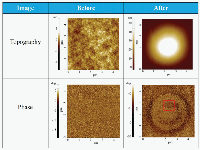
By way of comparison between the topography and phase image, it could be noted that the orientation of the lamellar fibrils in the inner and outer circular protrusions is reorganized and the fibrils are lined-up differently in both protrusions as well as the flat surface.
Figure 2a and 2b are the expanded view and comparable 3D representation of the area highlighted in red in the phase image of Table 1. Both images make it clear that there are particular differences in the fibril alignment.
The upper and lower part of Figure 2a therefore captures periodic fibrils aligning in-plane, while the dotted area in the center of the image relates to the domains with fibrils that are rearranged in the vertical direction throughout the heat and bias treatment.
Figure 2c is the corresponding line profile produced using Park XEI image analysis software to analyze the sizes of the lamellar fibrils as well as phase separation. The recorded width of the lamellar fibrils was around 26 nm, while separation between each fibril was roughly 22 nm.
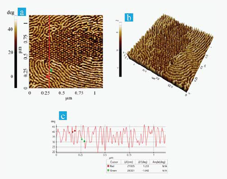
Figure 2. (a) Enlarged view of the phase image in table 1 (after heat and bias treatment), (b) 3D view of Figure 2a, (c) Corresponding line profileof Figure 2a. Image Credit: Park Systems
Summary
For the purpose of polymer thin film characterization, this study clearly illustrates the appropriateness of phase imaging. The high-resolution phase images acquired in the experiment displays considerable changes on the surface of the polymer thin films after they experienced heating and bias application.
It is noteworthy that throughout the heat and bias application, some polymer fibrils rearranged towards a vertical orientation while others remained in-plane. In addition, the in-plane fibrils created various domains of different orientations.
Phase imaging can therefore offer unparalleled insights into how temperature and DC voltage impact the fibril arrangement and orientation of polymer thin films, as necessary in the design of bespoke properties.
Since phase imaging functions in AFM tapping mode, this method enables the safe acquisition of high-resolution images without the continuous tip-sample contact.
In short, phase imaging is a tool with great promise in applications that demand high-resolution imaging of material contrasts on the nanoscale.
References
- S. Satish, et al., Preparation and characterization of nanoscale PMMA thin films Indian Journal of Pure & Applied Physics. Vol. 52, January 2014, pp. 64-67.
- V. Korolkov, et al., Ultra-high resolution imaging of thin films and single strands of polythiophene using atomic force microscopy. Nature Communications volume 10, Article number: 1537 (2019)
- J. Brostin, Compositional Imaging of Polymers Using a Field Emission Scanning Electron Microscope with a Microchannel Plate Backscattered Electron Detector. SCANNING Vol. 17, 327–329 (1995). Received March 13, 1995 and Accepted with revision May 22, 1995.
- R. Masters, et al., Sub-nanometre resolution imaging of polymer–fullerene photovoltaic blends using energy-filtered scanning electron microscopy. Nature Communications volume 6, Article number: 6928 (2015)
- https://www.parksystems.com/images/spmmodes/standard/3_Phase-Imaging-and-Phase- Detection-Microscopy-(PDM).pdf
- J. Gunther, Introduction to Atomic Force Microscopy, March 10, 1998, ACS Group and MENs, Beckman Institute. https://www.slideshare.net/joserabelo/atomic-force-microscopy-37962055

This information has been sourced, reviewed and adapted from materials provided by Park Systems.
For more information on this source, please visit Park Systems.
