Close Menu
  • News
  • Medical
  • Technology
  • Nanomaterials
  • Research
  • Blog
    • Nasiol.com
  • Contact
    • Tech7685@gmail.com
What's Hot

A new molecular model of bilayer graphene with higher semiconducting properties

May 31, 2025

5 Nanomaterial Innovations That Didn’t Deliver (Yet)

May 30, 2025

Scientists identify new 2D copper boride material with unique atomic structure

May 30, 2025
Facebook X (Twitter) Instagram
Nanotech – Nanomaterials | Medical | Research | News Stories Updated Daily Nanotech – Nanomaterials | Medical | Research | News Stories Updated Daily
  • News
  • Medical
  • Technology
  • Nanomaterials
  • Research
  • Blog
    • Nasiol.com
  • Contact
    • Tech7685@gmail.com
Facebook X (Twitter) Instagram
Nanotech – Nanomaterials | Medical | Research | News Stories Updated Daily Nanotech – Nanomaterials | Medical | Research | News Stories Updated Daily
Home»News»New synthesis technology for single-crystal 2D semiconductors could spawn next-generation devices
News

New synthesis technology for single-crystal 2D semiconductors could spawn next-generation devices

March 14, 2025No Comments4 Mins Read
Facebook Twitter Pinterest Telegram LinkedIn Tumblr WhatsApp Email
New synthesis technology for single-crystal 2D semiconductors could spawn next-generation devices
Share
Facebook Twitter LinkedIn Pinterest Telegram Email
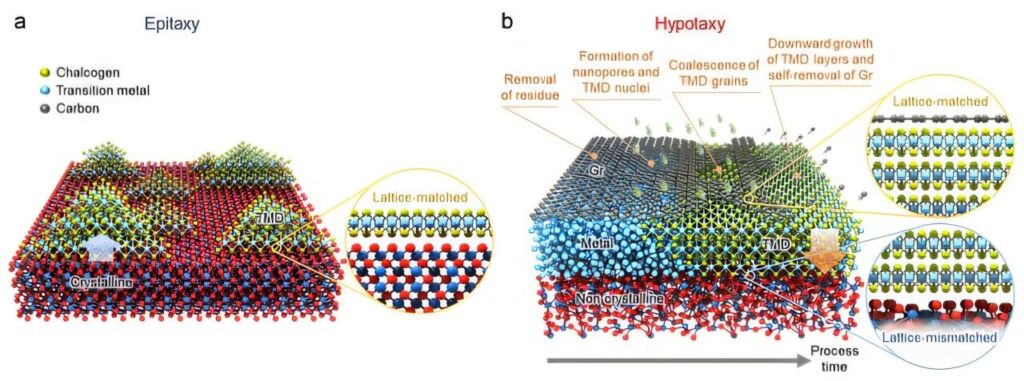
Schematic comparison between TMD growth via epitaxy and Hypotaxy. Credit: Nature (2025). DOI: 10.1038/s41586-024-08492-9

A research team has successfully developed a new synthesis technology for 2D semiconductors. This technique enables the direct growth of wafer-scale single-crystal 2D semiconductors on various substrates. The research is published in Nature.

With the advancement of artificial intelligence (AI) technology, the demand for enhanced semiconductor performance has increased, along with active research on reducing power consumption in semiconductor devices. As a result, new semiconductor materials to replace conventional silicon are gaining attention.

Among them, 2D materials such as transition metal dichalcogenides (TMDs) have been highlighted as next-generation semiconductors due to their thin structure and excellent electrical properties. However, there is currently a lack of mass production technology to synthesize them in high quality and utilize them industrially.

The most promising synthesis method to date, chemical vapor deposition (CVD), suffers from issues such as degradation of electrical properties and the necessity of transferring grown TMDs to different substrates, adding extra complexity to the process. Additionally, the “epitaxy” method, which grows TMDs on highly crystalline substrates, also requires a transfer process and is limited to specific substrates.

Consequently, the development of advanced 3D integration technology based on high-quality TMDs has emerged as a crucial challenge in the modern semiconductor industry, further emphasizing the urgent need for a novel TMD synthesis method.

To address this issue, the research team developed a completely new growth method. They introduced an approach that leverages 2D materials—such as graphene and hexagonal boron nitride—as templates, guiding TMD crystal alignment to enable the synthesis of perfectly single-crystalline TMD films on any substrate. This technique, named “hypotaxy,” was developed for the first time in the world. The name “hypotaxy” was derived by combining “hypo” (meaning “downward”) and “taxy” (meaning “arrangement”), reflecting the downward growth characteristic of the synthesized films.

SNU researchers develop a new synthesis technology of single crystal 2D semiconductors, "Hypotaxy," to enhance the commercialization of next-generation 2D semiconductors
(From top to bottom) Schematic representation of TMD growth progress over time, transmission electron microscopy (TEM) images, diffraction patterns, and cross-sectional TEM images of TMD growth using Hypotaxy. Credit: Nature (2025). DOI: 10.1038/s41586-024-08492-9

This technology holds significant industrial potential as it allows the growth of single-crystal TMDs at a low temperature (400°C), making it compatible with existing semiconductor manufacturing processes. Additionally, the graphene template naturally disappears without requiring a post-removal process, and the thickness of the metal film can be precisely controlled to regulate the number of TMD layers. These distinguishing features set hypotaxy apart from existing methods.

See also  High-Shear Mixing and High-Pressure Homogenization

Furthermore, semiconductor devices fabricated using TMDs synthesized through hypotaxy demonstrated high charge carrier mobility and excellent device uniformity, indicating that hypotaxy has great potential to contribute to the development of high-performance, high-integration 2D semiconductor devices and the commercialization of next-generation 2D semiconductors.

Discover the latest in science, tech, and space with over 100,000 subscribers who rely on Phys.org for daily insights.
Sign up for our free newsletter and get updates on breakthroughs,
innovations, and research that matter—daily or weekly.

Beyond its application in 2D semiconductor growth, hypotaxy is being recognized as an innovative technique applicable to the synthesis of all crystalline thin-film materials. By not only overcoming the limitations of traditional semiconductor fabrication methods but also enabling precise control over crystal orientation and structure through templating, this approach presents a groundbreaking method that has never been proposed before.

SNU researchers develop a new synthesis technology of single crystal 2D semiconductors, "Hypotaxy," to enhance the commercialization of next-generation 2D semiconductors
Nanopore-formed graphene via oxygen plasma and MoS2 synthesized at 400°C using this method. Credit: Seoul National University College of Engineering

Professor Gwan-Hyoung Lee, who led the research, emphasized the significance of the study, stating, “The hypotaxy technique that we have developed overcomes the limitations of epitaxy, a concept first proposed in the 1930s and a fundamental pillar of modern electronic device development. Since hypotaxy enables 3D integration, which is essential for next-generation AI semiconductors, I expect it will establish itself as a revolutionary approach in materials engineering.”

Donghoon Moon, the first author of the paper, reflected on the research process, saying, “The greatest challenge was breaking away from the conventional perception of epitaxy, which has been the standard for synthesizing various high-quality materials. Just as hypotaxy emerged from a counterintuitive perspective on epitaxy, I hope this achievement serves as a catalyst for groundbreaking research in areas such as new material development and the synthesis of novel lattice structures.”

See also  Revolutionary Graphene Interfaces Set to Transform Neuroscience

Provided by
Seoul National University


Source link

Devices NextGeneration semiconductors singlecrystal spawn Synthesis technology
Share. Facebook Twitter Pinterest LinkedIn Tumblr Email

Related Posts

A new molecular model of bilayer graphene with higher semiconducting properties

May 31, 2025

5 Nanomaterial Innovations That Didn’t Deliver (Yet)

May 30, 2025

Scientists identify new 2D copper boride material with unique atomic structure

May 30, 2025

Nanoscale biosensor lets scientists monitor molecules in real time

May 30, 2025

How should we govern nanotechnology?

May 29, 2025

The Future of Needle-Free Immunization

May 28, 2025

Comments are closed.

Top Articles
News

Ultrafast plasmon-enhanced magnetic bit switching at the nanoscale

News

The Role of Nano-catalysts in Biofuel Production

Modified glass fiber microstructure could illuminate blood vessel health from within

Editors Picks

A new molecular model of bilayer graphene with higher semiconducting properties

May 31, 2025

5 Nanomaterial Innovations That Didn’t Deliver (Yet)

May 30, 2025

Scientists identify new 2D copper boride material with unique atomic structure

May 30, 2025

New contact lenses allow wearers to see in the near-infrared

May 30, 2025
About Us
About Us

Your go-to source for the latest nanotechnology breakthroughs. Explore innovations, applications, and implications shaping the future at the molecular level. Stay informed, embrace the nano-revolution.

We're accepting new partnerships right now.

Facebook X (Twitter) Instagram Pinterest
Our Picks

TU Dresden researchers develop highly innovative solutions for the detection of viral pathogens

September 16, 2023

Scientists develop ultrafast hydrogen leak detection

February 3, 2024

Researchers develop neutron-shielding film for radiation protection

November 25, 2023

Subscribe to Updates

Get the latest creative Nano Tech news from Elnano.com

© 2025 Elnano.com - All rights reserved.
  • Contact
  • Privacy Policy
  • Terms & Conditions

Type above and press Enter to search. Press Esc to cancel.

Cleantalk Pixel