Semiconducting transition metal dichalcogenides (TMDs) are a class of layered materials exhibiting unique optoelectronic properties that could be leveraged to develop transistors, sensors and other nanoelectronics. Despite their advantages, creating robust ohmic contacts that connect a metal electrode in transistors to semiconducting TMDs at cryogenic temperatures has proved challenging.
This has so far limited the use of these materials for either studying fundamental physics or developing nanoelectronics that operate at low temperatures.
In a paper in Nature Electronics, researchers at the Liaoning Academy of Materials, Shanxi University and other institutes introduced a new technique for realizing ohmic contacts to the TMD molybdenum disulfide (MoS2) at cryogenic temperatures, and found that electron mobility in those transistors can be surprisingly high.
“For four decades, researchers have struggled to search for solid state 2D electron gas (2DEG) that exhibit fractionally quantized transverse conductance plateaus, with only a very limited number of them being reported, including quantum wells and graphene,” Zheng Vitto Han, senior author of the paper, told Phys.org.
“The search for fractional quantum Hall effects in new systems with high charge mobilities remains a fundamental yet challenging pursuit. Recently, spectra of Landau levels in 2D semiconductors, especially transition metal dichalcogenides, are intensively studied experimentally.”
While previous studies highlighted the potential of TMDs for realizing fractional quantum Hall phases, previous efforts only reported fractions above the quantum limit (i.e., with filling fractions greater than 1). As part of their research efforts, Han and his colleagues set out to tackle this unsolved research challenge.
“Correctly quantized fractional quantum Hall plateaus in TMDs, especially at the lowest Landau levels where electron interactions are the most pronounced, has been missing so far, mainly due to the challenges in obtaining ohmic contact at very low temperatures,” said Siwen Zhao, the first author of the paper. “We started working to fill this gap in the literature in early 2020.”
The main objective of the team’s recent study was to devise a viable strategy for realizing robust and reproducible Ohmic contacts connecting metal electrodes to MoS2, which worked at a broader range of temperatures. Their proposed method builds on a research group at MIT, who had found that bismuth (Bi) would be a good metal to combine with MoS2.
This previous group had realized contacts between Bi and MoS2 at temperatures down to 50K. After various attempts, Han and his colleagues were able to devise an approach to reach below this temperature, thus extending the temperature range further.
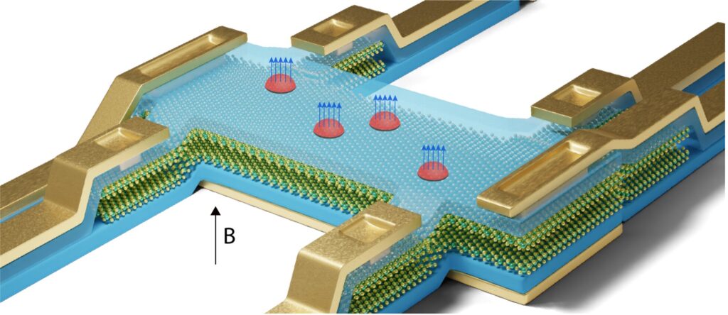
The strategy they used to achieve this has three main steps. These include the encapsulation of hexagonal boron nitride (h-BN) layers, the realization of a windowed contact and the thermal evaporation of Bi.
Discover the latest in science, tech, and space with over 100,000 subscribers who rely on Phys.org for daily insights.
Sign up for our free newsletter and get updates on breakthroughs,
innovations, and research that matter—daily or weekly.
“The high-mobility n-type molybdenum disulfide transistors, unlike conventional epitaxially-grown quantum well system, are made by simply stacking several van der Waals materials in sequence,” explained Jianming Lu, one of the leading authors.
“The first is an h-BN layer (a few nm in thickness), patterned with about 1×1 um windows, and then used to pick up the MoS2 layer (monolayer or a few layers) in a glove box. Second, the windowed-BN/MoS2 stack are deposited onto another BN flake, so that the MoS2 is encapsulated like a sandwich—but with nm thickness.”
After they completed these steps, the researchers processed the whole stack they created using a standard lithographic technique. They then metallized electrodes in the transistors they created and tested the resulting device’s performance.
Han and his colleagues found that the MoS2-based transistors they created exhibited Ohmic IV curves ranging from 300K to 50 mK. Moreover, the devices presented a remarkable electron mobility of over 100,000 cm2/V/s at cryogenic temperatures. It further allows the observation of fractional quantum Hall phases under a magnetic field of 34 T at a temperature of 300 mK.
“The fractional quantum Hall effect in our device relies on the alliance of topology and interactions leading to the emergence of quasi-particles that have no equivalent among the elementary particles,” said Nicolas Regnault, one of the leading authors.
“Some of these quasi-particles have been envisioned as a way to perform quantum computing with built-in error corrections. At a fundamental level, we still don’t know precisely if and which types of quasi-particles depending on electrons interact between each other in a material.”
The methods outlined in the recent paper by Han and their colleagues could open new possibilities for the realization of low temperature nanoelectronics based on the TMD MoS2. In the future, it could inspire other research groups to employ similar techniques to realize ohmic contacts enabling the free flow of electrons between metal and TMDs at low temperatures.
“Being able to observe the fractional quantum Hall effect in our samples is a benchmark for the quality of the devices that can be envisioned in the near future,” said Ning Wang, one of the leading authors.
“We now plan to explore various research directions. First, the valley-layer locked, and fully valley- and spin-polarized Landau levels, hence the flavors that affect the FQH phases, in MoS2 are unique compared to other materials systems (actually, there are so far only graphene and semiconducting quantum wells). It might allow the tuning of the FQH states via a totally new tuning knob—such as the polarized light, which could never be possible in neither quantum wells, nor graphene,” added Jing Zhang, one of the leading authors.
In their next studies, Han and his colleagues also plan to explore other potential applications of their experimental findings. For instance, based on the high performance of the TMD transistors at mK temperatures, their strategy could enable the development of low temperature nanoelectronics such as cryogenic logic circuits that could support the operation of quantum technologies.


