Close Menu
  • News
  • Medical
  • Technology
  • Nanomaterials
  • Research
  • Blog
    • Nasiol.com
  • Contact
    • Tech7685@gmail.com
What's Hot

Deep-trench 3D printing enables next-gen RF devices with unprecedented precision

May 12, 2025

Large-aperture MEMS modulator paves way for high-speed, energy-efficient optical communication systems

May 11, 2025

Dual-stage monitoring technique for nanocomposites can streamline manufacturing and property tracking

May 11, 2025
Facebook X (Twitter) Instagram
Nanotech – Nanomaterials | Medical | Research | News Stories Updated Daily Nanotech – Nanomaterials | Medical | Research | News Stories Updated Daily
  • News
  • Medical
  • Technology
  • Nanomaterials
  • Research
  • Blog
    • Nasiol.com
  • Contact
    • Tech7685@gmail.com
Facebook X (Twitter) Instagram
Nanotech – Nanomaterials | Medical | Research | News Stories Updated Daily Nanotech – Nanomaterials | Medical | Research | News Stories Updated Daily
Home»News»New crystal production method could enhance quantum computers and electronics
News

New crystal production method could enhance quantum computers and electronics

May 31, 2024No Comments4 Mins Read
Facebook Twitter Pinterest Telegram LinkedIn Tumblr WhatsApp Email
New crystal production method could enhance quantum computers and electronics
Share
Facebook Twitter LinkedIn Pinterest Telegram Email
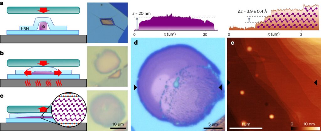
Growth of ultrathin bismuth crystals inside a vdW mold. a–c, Cross-sectional schematics of the vdW-mold process with corresponding optical images of the bismuth. a, Bismuth flake encapsulated in hBN on a bottom substrate of Si/SiO2 before squeezing. b, Uniaxial compression (vertical red arrow) is applied to the stack by a rigid top substrate (glass or sapphire) while the stage is heated. When the bismuth reaches its melting point, it rapidly compresses and expands laterally. c, Bismuth is cooled below its melting point and then pressure is removed, resulting in an ultrathin bismuth crystal. The inset shows the atomic structure. d, Optical image of the encapsulated vdW-molded bismuth (sample M30); black triangles indicate location of the AFM line trace (top) of the bismuth taken after removing the top hBN flake. This bismuth varies from 10 to 20 nm thick. e, AFM topography of the vdW-molded bismuth after removing the top hBN, showing wide flat terraces. Black triangles show location of the line trace (top). The average step height is 3.9 ± 0.4 Å. The diagram inset in the shaded region shows the crystal structure. Credit: Nature Materials (2024). DOI: 10.1038/s41563-024-01894-0

In a study published in Nature Materials, scientists from the University of California, Irvine describe a new method to make very thin crystals of the element bismuth—a process that may aid the manufacturing of cheap flexible electronics an everyday reality.

“Bismuth has fascinated scientists for over a hundred years due to its low melting point and unique electronic properties,” said Javier Sanchez-Yamagishi, assistant professor of physics & astronomy at UC Irvine and a co-author of the study. “We developed a new method to make very thin crystals of materials such as bismuth, and in the process reveal hidden electronic behaviors of the metal’s surfaces.”

The bismuth sheets the team made are only a few nanometers thick. Sanchez-Yamagishi explained how theorists have predicted that bismuth contains special electronic states allowing it to become magnetic when electricity flows through it—something essential for quantum electronic devices based on the magnetic spin of electrons.

One of the hidden behaviors observed by the team is so-called quantum oscillations originating from the surfaces of the crystals.

“Quantum oscillations arise from the motion of an electron in a magnetic field,” said Laisi Chen, a Ph.D. candidate in physics & astronomy at UC Irvine and one of the lead authors of the paper. “If the electron can complete a full orbit around a magnetic field, it can exhibit effects that are important for the performance of electronics. Quantum oscillations were first discovered in bismuth in the 1930s, but have never been seen in nanometer-thin bismuth crystals.”

Amy Wu, a Ph.D. candidate in physics in Sanchez-Yamagishi’s lab, likened the team’s new method to a tortilla press. To make the ultra-thin sheets of bismuth, Wu explained, they had to squish bismuth between two hot plates. To make the sheets as flat as they are, they had to use molding plates that are perfectly smooth at the atomic level, meaning there are no microscopic divots or other imperfections on the surface.

See also  A simple, scalable method using light to 3D print helical nanostructures

“We then made a kind of quesadilla or panini where the bismuth is the cheesy filling and the tortillas are the atomically flat surfaces,” said Wu.

“There was this nervous moment where we had spent over a year making these beautiful thin crystals, but we had no idea whether its electrical properties would be something extraordinary,” said Sanchez-Yamagishi. “But when we cooled down the device in our lab, we were amazed to observe quantum oscillations, which have not been previously seen in thin bismuth films.”

“Compression is a very common manufacturing technique used for making common household materials such as aluminum foil, but is not commonly used for making electronic materials like those in your computers,” Sanchez-Yamagishi added. “We believe our method will generalize to other materials, such as tin, selenium, tellurium and related alloys with low melting points, and it could be interesting to explore for future flexible electronic circuits.”

Next, the team wants to explore other ways in which compression and injection molding methods can be used to make the next computer chips for phones or tablets.

“Our new team members bring exciting ideas to this project, and we’re working on new techniques to gain further control over the shape and thickness of the grown bismuth crystals,” said Chen. “This will simplify how we fabricate devices, and take it one step closer for mass production.”

The research team included collaborators from UC Irvine, Los Alamos National Laboratory and the National Institute for Materials Science in Japan.

Provided by
University of California, Irvine


See also  A New Method for Non-invasive or Inline Detection of Aggregates and Oversized Particles in Nanosuspensions


Source link

Computers crystal Electronics Enhance method Production quantum
Share. Facebook Twitter Pinterest LinkedIn Tumblr Email

Related Posts

Deep-trench 3D printing enables next-gen RF devices with unprecedented precision

May 12, 2025

Large-aperture MEMS modulator paves way for high-speed, energy-efficient optical communication systems

May 11, 2025

Dual-stage monitoring technique for nanocomposites can streamline manufacturing and property tracking

May 11, 2025

Probing the molecular mechanisms of metastasis

May 10, 2025

AI-powered electronic nose detects diverse scents for health care and environmental applications

May 10, 2025

Microbubble dynamics in boiling water enable precision fluid manipulation

May 9, 2025

Comments are closed.

Top Articles
Technology

Inhalable nanoparticles could help treat chronic lung disease

News

Deep learning system detects disease-related nanoparticles

Probing the molecular mechanisms of metastasis

Editors Picks

Deep-trench 3D printing enables next-gen RF devices with unprecedented precision

May 12, 2025

Large-aperture MEMS modulator paves way for high-speed, energy-efficient optical communication systems

May 11, 2025

Dual-stage monitoring technique for nanocomposites can streamline manufacturing and property tracking

May 11, 2025

Probing the molecular mechanisms of metastasis

May 10, 2025
About Us
About Us

Your go-to source for the latest nanotechnology breakthroughs. Explore innovations, applications, and implications shaping the future at the molecular level. Stay informed, embrace the nano-revolution.

We're accepting new partnerships right now.

Facebook X (Twitter) Instagram Pinterest
Our Picks

The Promise and Potential of Nanotechnology Investments

December 6, 2023

UCLA Study Challenges Long-Held Beliefs in Bioengineering and Stem Cell Dynamics

December 27, 2023

Light-driven method creates molecular fit that would otherwise be impossible

January 6, 2025

Subscribe to Updates

Get the latest creative Nano Tech news from Elnano.com

© 2025 Elnano.com - All rights reserved.
  • Contact
  • Privacy Policy
  • Terms & Conditions

Type above and press Enter to search. Press Esc to cancel.

Cleantalk Pixel