Close Menu
  • News
  • Medical
  • Technology
  • Nanomaterials
  • Research
  • Blog
    • Nasiol.com
  • Contact
    • Tech7685@gmail.com
What's Hot

A new molecular model of bilayer graphene with higher semiconducting properties

May 31, 2025

5 Nanomaterial Innovations That Didn’t Deliver (Yet)

May 30, 2025

Scientists identify new 2D copper boride material with unique atomic structure

May 30, 2025
Facebook X (Twitter) Instagram
Nanotech – Nanomaterials | Medical | Research | News Stories Updated Daily Nanotech – Nanomaterials | Medical | Research | News Stories Updated Daily
  • News
  • Medical
  • Technology
  • Nanomaterials
  • Research
  • Blog
    • Nasiol.com
  • Contact
    • Tech7685@gmail.com
Facebook X (Twitter) Instagram
Nanotech – Nanomaterials | Medical | Research | News Stories Updated Daily Nanotech – Nanomaterials | Medical | Research | News Stories Updated Daily
Home»News»Neatly arranging crystal growth to make fine thin films
News

Neatly arranging crystal growth to make fine thin films

August 27, 2024No Comments2 Mins Read
Facebook Twitter Pinterest Telegram LinkedIn Tumblr WhatsApp Email
Neatly arranging crystal growth to make fine thin films
Share
Facebook Twitter LinkedIn Pinterest Telegram Email
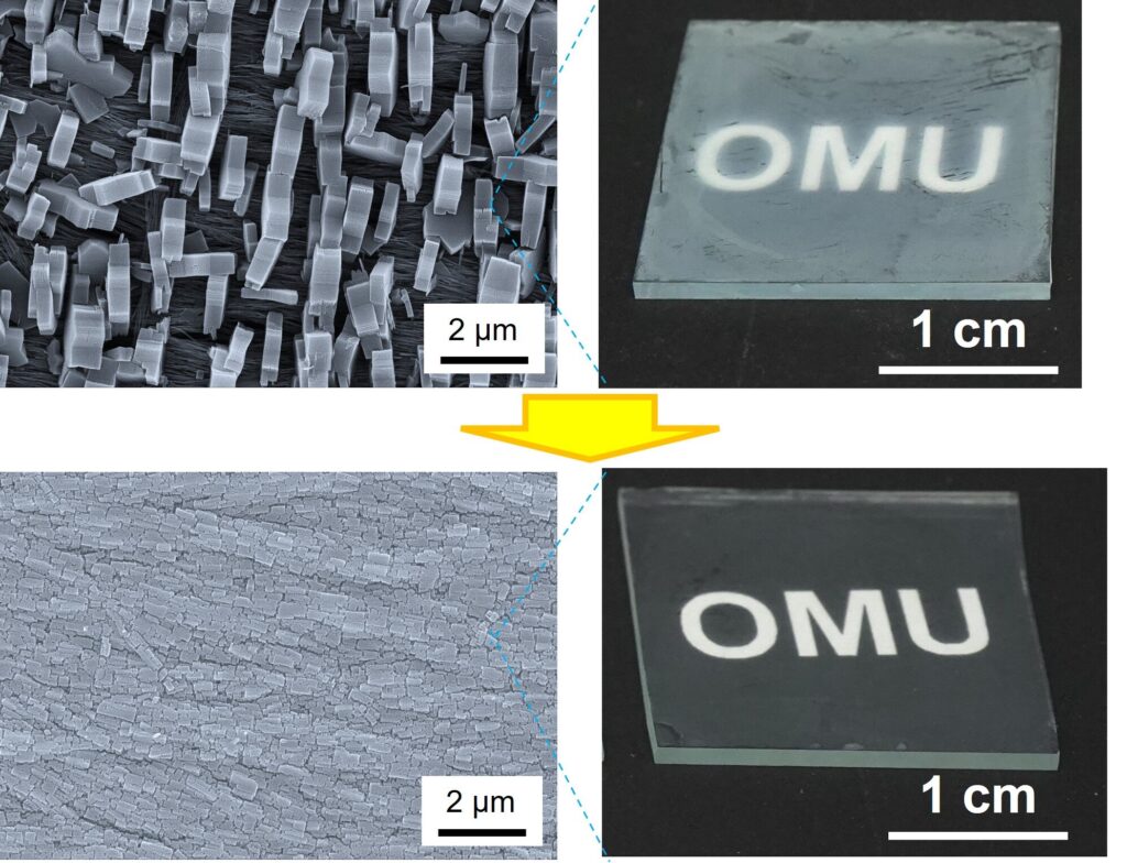
The metal-organic framework thin film synthesized at top did not involve a modulator, while the finely arranged version above did. Credit: Osaka Metropolitan University

Table salt and refined sugar look white to our eyes, but that is only because their individual colorless crystals scatter visible light. This feature of crystals is not always desirable when it comes to materials for optical and electrical devices, however.

Metal-organic frameworks are one such material. Crystalline with micropores, thin films of these nanomaterials have been attracting attention as a next-generation material that could also have an impact on environmental issues such as hydrogen storage and carbon dioxide capture.

An Osaka Metropolitan University Graduate School of Engineering team has found a way to control the growth of crystals on such thin films so that light scattering is reduced significantly.

The findings were published in Nanoscale.

Associate Professor Kenji Okada and Professor Masahide Takahashi led the team in developing a technique for forming thin films on substrates by having the crystals grow in an orderly manner through the use of a modulator. A mixture of diluted acetic acid, the main acid of vinegar, and sodium acetate made up the modulator, which interacted with the copper-based medium to grow crystals in only one direction.

By arranging the crystals neatly without gaps, the team succeeded in fabricating a thin film of unprecedented high quality.

“The thin films fabricated in this research have numerous molecular-sized pores that allow light to pass through them well,” Professor Okada explained. “They are expected to be used as optical sensors, optical elements, and transparent gas adsorption sheets that utilize the change in optical properties during molecular adsorption.”

Provided by
Osaka Metropolitan University


See also  Butterfly-Inspired Films Create Vibrant Colors While Passively Cooling Objects


Source link

arranging crystal Films fine growth Neatly thin
Share. Facebook Twitter Pinterest LinkedIn Tumblr Email

Related Posts

A new molecular model of bilayer graphene with higher semiconducting properties

May 31, 2025

5 Nanomaterial Innovations That Didn’t Deliver (Yet)

May 30, 2025

Scientists identify new 2D copper boride material with unique atomic structure

May 30, 2025

Nanoscale biosensor lets scientists monitor molecules in real time

May 30, 2025

How should we govern nanotechnology?

May 29, 2025

The Future of Needle-Free Immunization

May 28, 2025

Comments are closed.

Top Articles
News

The Future of On-chip Optical Communication

News

A Guide to Semiconductor Chip Layers

News

Plasma-synthesized photothermal material could enable efficient solar-powered water purification

Editors Picks

A new molecular model of bilayer graphene with higher semiconducting properties

May 31, 2025

5 Nanomaterial Innovations That Didn’t Deliver (Yet)

May 30, 2025

Scientists identify new 2D copper boride material with unique atomic structure

May 30, 2025

New contact lenses allow wearers to see in the near-infrared

May 30, 2025
About Us
About Us

Your go-to source for the latest nanotechnology breakthroughs. Explore innovations, applications, and implications shaping the future at the molecular level. Stay informed, embrace the nano-revolution.

We're accepting new partnerships right now.

Facebook X (Twitter) Instagram Pinterest
Our Picks

A Comparative Analysis for Material Identification and Reaction Monitoring

August 17, 2024

Sensor technology uses nature’s blueprint and machinery to monitor metabolism in body

April 4, 2025

MIT Engineers Create Game-Changing Lead Detection Device

May 17, 2024

Subscribe to Updates

Get the latest creative Nano Tech news from Elnano.com

© 2025 Elnano.com - All rights reserved.
  • Contact
  • Privacy Policy
  • Terms & Conditions

Type above and press Enter to search. Press Esc to cancel.

Cleantalk Pixel