


From materials science to biotechnology, the field of nanotechnology has branched out into various areas of research. Several of these applications are predicated on the capacity to fabricate or manipulate nanostructured materials [1].
Atomic force microscopy (AFM) nanolithography is an appropriate method for structuring, manipulation and fabrication at the nanometer scale. There are two common groups of AFM nanolithography techniques relative to their operational principles: bias-assisted and force-assisted nanolithography [2].
By applying a large force to a sharp tip to mechanically alter the surface atoms or molecules of the sample and generate surface trenches, the force-assisted method is achieved. In this case, the interaction between the tip and the sample is strictly mechanical [2].
The bias-assisted method requires the application of a voltage between the AFM tip and the substrate connecting the sample. The tip-sample voltage induces an electrochemical reaction that generates an oxide on the substrate’s surface [1].
This application note outlines an electrochemical process known as anodic oxidation utilizing the bias-assisted lithography method to produce oxide patterns on the surface of a silicon substrate.
The success of this technique depends on using the AFM tip as a biased cathode to the sample surface. The size of the water meniscus around the sample is directly influenced by the environment humidity [1] and it works as an electrolyte for the chemical reaction.
This application demonstrates nanoscale oxide line formation utilizing AFM anodized lithography on a Park NX10 AFM system using Park SmartLithoTM, the latest nanolithography software developed by Park Systems.
As well as nanomanipulation, Park SmartLitho can also be employed for scratching techniques and high voltage lithography [3].
Experimental
Nanopatterns were drawn onto a bare silicon substrate using a Park NX10 AFM in order to conduct bias-assisted nanolithography in this experiment. Park SmartLithoTM was used to create the oxide patterns.
Non-contact mode imaging was performed subsequent to the lithography process to validate the successful fabrication of the oxide patterns on the surface as well as distinguishing the surface difference between the oxide layers and silicon substrate.
Throughout these experiments, there the use of a conductive AFM cantilever probe (Multi 75G) with a nominal spring constant (k = 3 N/m) and resonance frequency (f = 75 kHz).
Figure 1. Park SmartLithoTM software. A) Vision & Monitoring view. B) Nanolithography mode panel. C) Lithography design area. D) Object list. E) Objects edit panel. Image Credit: Park Systems
The Park SmartLitho is primarily made up of five windows and panels that enable the operator to control the whole lithography process (Figure 1). The relevant alignment of the position-sensitive photodetector (PSPD) and super-luminescent diode (SLD) is confirmed (Figure 1A) in the first step.
The operator selects the control mode once the correct alignment has been confirmed; in this instance, the setpoint mode was chosen. For the anodic oxidation, a bias must be applied. Here, the tip was selected as the desired channel (Figure 1B).
Using a previous AFM image as a baseline in the design area (Figure 1C), the operator can add the desired shapes and figures and the embedded figures will emerge in the object list (in this instance, just one line) (Figure 1D).
The formation order can be modified by the operator and the approximate lithography time for each figure is presented.
Finally, parameters can be modified in the object edit panel (Figure 1E) for any desired feature. To acquire different features within the same designed figures, parameters such as load force, extend speed, stroke speed, lift speed, or voltage can be adjusted.
A baseline image is necessary to initiate a lithography or manipulation process. In this instance, the baseline image contains one previously-drawn line to contrast against the line about to be drawn (Figure 1C): the image is 1.5 µm by 1.5 µm.
In line with the image captured using non-contact AFM mode, the sample contains small nanoparticles on its surface.
Planning of the lithography process is conducted by utilizing the software to draw a shape on the surface. Park SmartScanTM, the AFM operating software, gives the operator easy positioning features and offset.
Contact mode is used to carry out the DC bias lithography process, and in this instance, a bias of negative 5.0 Volts is used between the sample and the tip. For this experiment, a line was drawn at 0.2 µm/s with a 200 nN load force.
The process is completed in just a couple of seconds and the drawn line is around 1.8 microns in length (Figure 2, Top Left). As the cantilever is compressed to the loading force of 200 nN, the PSPD signal moves up, which visually confirmed the pressure applied.
Results and Discussion
Subsequent to the lithography process and utilizing Park SmartScan, the system is changed to non-contact mode. Attached to the AFM head Z piezoelectric scanner, an AFM cantilever probe is positioned on a piezoelectric bimorph shaker.
The shaker vibrates the AFM cantilever probe at its resonant frequency, which is selected automatically along with the vibration amplitude. As the probe approaches the sample surface, the vibration amplitude reduces. Similarly, as the probe moves away from the surface, there is an increase in amplitude.
The Z piezo scanner moves up and down and alters its height to sustain a constant vibration amplitude. The height adjustment of the scanner reflects the change in height on the sample surface.
The AFM raster scans and identifies the height change point-by-point in the XY-direction to map out the surface topography in three-dimensions. The tip approaches the surface, and the image is recaptured immediately with the same parameters as the baseline AFM image.
The newly drawn line is displayed clearly and parallel to the drawn line previously (Figure 2, Top Left). Note, the image position stays the same, exhibiting the control of the XY-scanner, separate from the Z-scanner, even at reduced scan sizes.
In this instance, the lithography process is performed in contact mode, and therefore, imaging in non-contact mode is an option. Yet, post-manipulation, it is crucial to capture the image using non-contact mode to prevent a disturbance in the particles present on the sample.
After confirming the success of the lithography process, the last image is captured and exported to the analysis software named Park XEI™ [4]. In this experiment, it can be observed that the previously-drawn line is approximately 35 nm in width, and the newly-drawn one is 47 nm (Figure 2, Bottom).
Both lines are produced utilizing the same lithography parameters. Still, the line on the right side, the first drawn line, is seen to be narrower than the oxide line on the left. This could be due to carrying out the lithography in contact mode.
In contact mode, the tip rubs against the sample surface as the lines are generating. The rubbing can lead to blunting and excessive wear of the end of the tip. Consequently, the blunted tip draws wider oxide lines than the ones drawn with a sharper tip [1,5].
It is clear to see that the resulting line-height is around 1.4 nm for both lines when introducing an additional cursor. Park XEI software has the capacity to show a three-dimensional rendering of the image captured (Figure 2, Top Right).
With the 3D representation, it is discerned that the lines produced during this oxide growth process have a height reduction when compared to the nanoparticles on the surface.
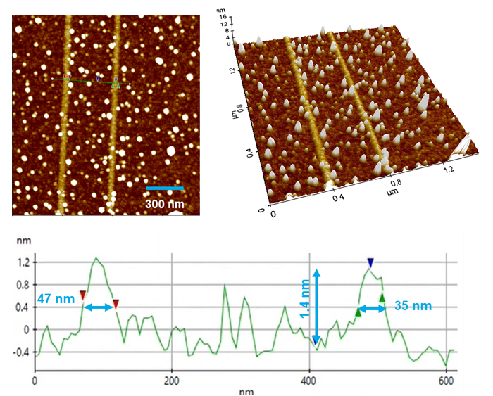
Figure 2. Nanolithography process. (Top Left) Post-scan image. Top Right) 3D View. (Bottom) Line profile plotted of green line seen in Top Left. Image Credit: Park Systems
Conclusion
This application note outlines how to use Park SmarthLithoTM software to design and customize nanoscale oxide patterns with ease while using Park NX10 AFM.
With a short runtime, mere seconds, this straightforward test case exhibits a bias-assisted nanolithography process, which generates oxide patterns as narrow as 35 nm in width successfully.
Although the process itself utilizes contact mode, true non-contact mode pre- and post-operation confirms that the new oxide line is, in fact, parallel to the line in the baseline image. This test case also determines the scanning and imaging accuracy of Park’s XY-scanner.
Overall, this study demonstrates that bias mode in Park SmartLitho software is a superior tool for producing well-defined nanoscale patterns and features.
References
- E. Pinilla-Cienfuegos, et al. Local Oxidation Nanolithography on Metallic Transition Metal Dichalcogenides Surfaces. Applied Science, (2016): 250.
- JP. Pineda, et al., Nanoscale material patterning using atomic force microscopy nanolithography. NanoScientific, Vol 18, (2020): 21-23.
- Park Systems. (2020). Park SmartScanTM. California, USA. https://parksystems.com/products/operating-software/park-smartscan
- Park Systems. (2020). XEI Data Processing and Analysis. California, USA. https://parksystems.com/manuals-software
- J. Voves. Nanoelectronics and nanolithography. Nanocon 20, (2009): 22-30.
This information has been sourced, reviewed and adapted from materials provided by Park Systems.
For more information on this source, please visit Park Systems.
