


The development of nanoelectronics has enabled operations at the nanoscale, resulting in the creation of smaller and more efficient electronic devices. Here, we offer a comprehensive summary of the methods utilized in manufacturing nanoelectronics, with a particular emphasis on lithography techniques, which have contributed significantly to the advancement of electronics since their inception.
Image Credit: IM Imagery/Shutterstock.com
Nanoelectronics Fabrication – Conventional Methods
The fabrication of nanoelectronics involves the integration of the technologies used to create small structures within the range of 1–100 nm. These structures can be incorporated into complex hierarchical systems. Typically, nanoelectronics fabrication employs both top-down and bottom-up methods.
In the top-down method, nanomaterials are obtained by removing the material from the bulk substrate until a desired structure is formed. This category includes printing methods. By contrast, the bottom-up method involves building a nanomaterial at the atomic or molecular level and gradually assembling it until the desired structure is achieved.
Commonly used methods for creating nanoelectronics involve lift-off, stamping, and stripping for transfer, molecular-scale devices, self-assembly, and processes such as electroplating and vacuum metal deposition.
What is Lithography?
Lithography involves creating a precise and repeatable pattern on a specialized layer of material placed on a substrate through chemical modification. This pattern is transferred to another layer using conventional etching or lift-off techniques. Lithography is a crucial aspect of the ongoing nanotechnology revolution that has enabled the development of smaller and more advanced semiconductor devices with consistently decreasing dimensions.
Advantages of Lithography Over Conventional Methods
Modern integrated circuits (IC) are multi-component, multilevel nanostructures comprising memory, logic processors, and analog devices prepared using a series of patterning and pattern-transfer steps. Three-dimensional (3D) nanoelectronic structures are manufactured using lithography, a rapid patterning process.
Lithography has enabled the semiconductor industry to reduce its dimensions continually. Moore first quantified the early progress of this technology in 1965, and it is now known as Moore’s Law. To achieve ongoing miniaturization of electronic components, it is essential to make advancements in all aspects of the manufacturing process. However, improvements in lithography have played a significant role in this process.
Moore’s Law has been instrumental in driving the consistent enhancement of transistors per chip in the semiconductor industry, starting from the inception of the IC. Over the years, several lithography techniques have been devised, with optical steps and repeat lithography emerging as the primary methods for patterning features onto semiconductor surfaces and overlying interconnected structures.
Although other competing technologies, such as X-rays and flood electron beams, have been explored, optical lithography has remained dominant because of vigorous optical technology and tool developments that have made it the lowest-cost solution with the highest throughput.
Recent Advancements in Lithography for Nanoelectronics Fabrication
Advances in next-generation lithography techniques, including nanoimprint lithography (NIL), photolithography, and ultraviolet (UV)-curable nanoimprint lithography, have enabled the production of smaller structures, enhancement of the properties of organic resists and expansion of industrial applications, thereby benefiting the field of nanoelectronics.
NIL has emerged as a low-cost, high-resolution, and versatile alternative to optical lithography for patterning nanoelectronic devices for semiconductor fabrication and other applications. NIL relies on a simple squeeze flow mechanism in which a resist flows into a well-defined physical cavity with nanoscale dimensions.
In contrast to optical lithography, which requires tight control of the environmental conditions for every printing or copy of the nanostructured surface, NIL’s resolution of NIL is largely controlled by the quality of the imprint master.
The use of UV-NIL in nanoelectronics fabrication is advantageous because of its ability to meet low-pressure, room-temperature, and high-throughput requirements. However, defects in the resist pattern remain a challenge for mass production.
The demolding process, which separates the mold from the cured resist during nanoimprinting, is the primary source of the pattern defects. This is because of the strong adhesion between the mold and resist, which results from the volume shrinkage of the UV-curable resist during polymerization. This shrinkage can cause defects in the resist pattern during the demolding. UV-curable nanoimprint resists typically consist of resin monomers, photoinitiators, and additives.
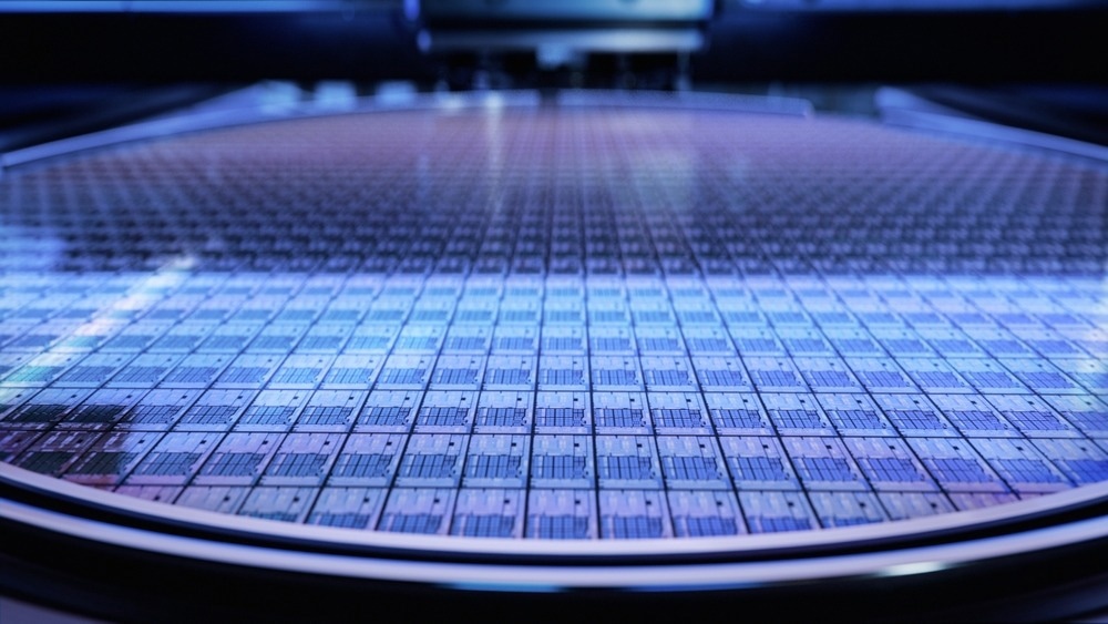
Image Credit: IM Imagery/Shutterstock.com
Lithography Techniques and Their Commercial Applications
All types of lithography have unique advantages that render them suitable for various nanoelectronic applications. For instance, photolithography is a cost-effective and high-throughput method that is commonly used in nanoelectronics for large-scale manufacturing. In contrast, extreme UV lithography (EUVL) is a complex and expensive technique crucial for the manufacture of next-generation semiconductor devices with feature sizes ≤ 5 nm.
Despite its slow production speed, electron beam lithography is an excellent option because of its exceptional resolution and versatility, making it ideal for research, prototyping, and specialized equipment in photonics and quantum computing.
Both NIL and X-ray lithography can produce high-resolution patterns across large areas in a single step, making them appealing for creating repeating patterns. Of these two methods, NIL has been particularly successful in applications such as nanoelectronics, photonics, and data storage.
On the other hand, focused ion beam lithography is a potent tool for creating novel nanoscale devices and structures, especially in research settings, owing to its ability to add and remove materials.
Conclusion
Overall, nanoelectronic fabrication involves the creation of small structures in the 1-100 nm range using top-down and bottom-up methods, including lift-off, stamping, self-assembly, electroplating, and vacuum metal deposition.
Lithography plays a crucial role in the manufacturing of 3D nanoelectronic structures, and Moore’s Law relies heavily on advancements in this field. Although X-ray and electron beam technologies have been explored, optical lithography remains the dominant method, owing to its cost-effectiveness and high throughput.
Recent advances in lithography, such as nanoimprint lithography (NIL) and UV-curable nanoimprint lithography, offer high resolution and versatility. However, challenges remain concerning the defects in resist patterns during demolding.
Different lithography techniques have unique strengths: photolithography is cost-effective for large-scale manufacturing, EUVL is crucial for sub-5 nm devices, electron beam lithography offers exceptional resolution for research and specialized applications, and NIL and X-ray lithography excels in high-resolution patterning. Focused Ion Beam Lithography is powerful for creating novel nanoscale devices in research settings.
Thus, lithography, especially with recent advancements such as NIL, remains a cornerstone in nanoelectronics fabrication, offering a range of methods to meet different manufacturing needs and applications.
Two-Photon Lithography: A Review
References and Further Reading
Shi, X., & Boden, S. A. (2016). Scanning helium ion beam lithography. In Frontiers of Nanoscience. 11, 563-594. Elsevier. https://doi.org/10.1016/B978-0-08-100354-1.00017-X
Ronse, K. (2017). Lithography for Nanoelectronics. Nanoelectronics: Materials, Devices, Applications, 289-316. https://doi.org/10.1002/9783527800728.ch12
Knight, S., et al (2010) Nanoelectronics Lithography. [Online]
AZoNano (2014) Nanoscale Lithography Technologies. [Online]
