Molybdenene is a two-dimensional (2D) Dirac elemental material composed of only molybdenum (Mo) atoms. Hybridization of electron-rich molybdenene with 2D hexagonal boron nitride (h-BN) or molybdenum disulfide (MoS2) fetches tunable electronic and optical properties. This article offers a summary of molybdenene and its properties.
Image Credit: Peter Hermes Furian/Shutterstock.com
2D and Dirac Materials
2D materials are promising candidates in the fields of photonics and electronics. However, the presence of contaminants in the structural phases can hamper the unique potential of these materials. In contrast to other 2D materials, Dirac-like materials do not suffer from such contaminants and offer enhanced electronic mobilities.
Borophene, silicene, 2D gold, and graphene are a few known elemental Dirac materials that are non-metallic. Further advancements to include metallic elements such as tungsten (W), Mo, and titanium (Ti) can confine a sea of electrons to two dimensions, potentially leading to unprecedented excitonic and electronic behaviors.
Moreover, metallic Dirac materials retain their structural integrity even under high-stress environments such as high temperatures and pressures. Transition metals such as Mo exhibit variable oxidation states and desirable properties required to catalyze chemical reactions. Hence, transition metal-based atomic sheets show high catalytic activity.
Scanning tunneling microscopy tips, field emitters, surface-enhanced Raman spectroscopy (SERS)-based molecular sensing, nanoelectromechanical systems, and nanoscale interconnects are a few areas in which transition-metal-based 2D materials can be exploited. However, their affinity towards oxygen and tendency to form clusters makes their growth at ambient temperature challenging.
Molybdenene – A Graphene-Like Dirac Material
Graphene’s discovery has garnered notable attention due to its enhanced ability to conduct electricity and heat compared to copper and its high stability compared to steel. In addition, graphene is exceptionally light and flexible. The 2D structure of graphene also imparts unusual electromagnetic effects, opening avenues for groundbreaking innovations in quantum technology.
A collaborative study by research groups from the Indian Institute of Technology, India, The University of Newcastle, Australia, and the Institute of Electrochemistry and Energy Systems, Bulgaria, led to the fabrication of a novel, free-standing, metallic 2D material composed of only Mo atoms and was termed as “Molybdenene.”
This study was published in Nature Nanotechnology. The fabricated molybdenum sheet of atomic thickness was structurally similar to graphene, the best-known 2D material constituting carbon.
Molybdenene – Preparation and Structural Characteristics
In this study, molybdenene was prepared using MoS2 as the precursor, and its growth was induced using an electric field under microwave irradiation. Observation of the prepared material under field emission scanning electron microscopy (FESEM) revealed millimeter-long whiskers.
The whiskers appeared as a layered material with a large surface area, indicating weakly bonded molybdenene sheets. Exfoliation of the sheet with Scotch tape resulted in a metallic material with an electrical conductivity of approximately 940 S m−1. Observation of the sheets by atomic force microscopy (AFM) revealed the formation of screw-dislocation-mediated staircase-like growth at the edges with a step height of 0.4 nm.
Application of Molybdenene as Microscope Cantilevers
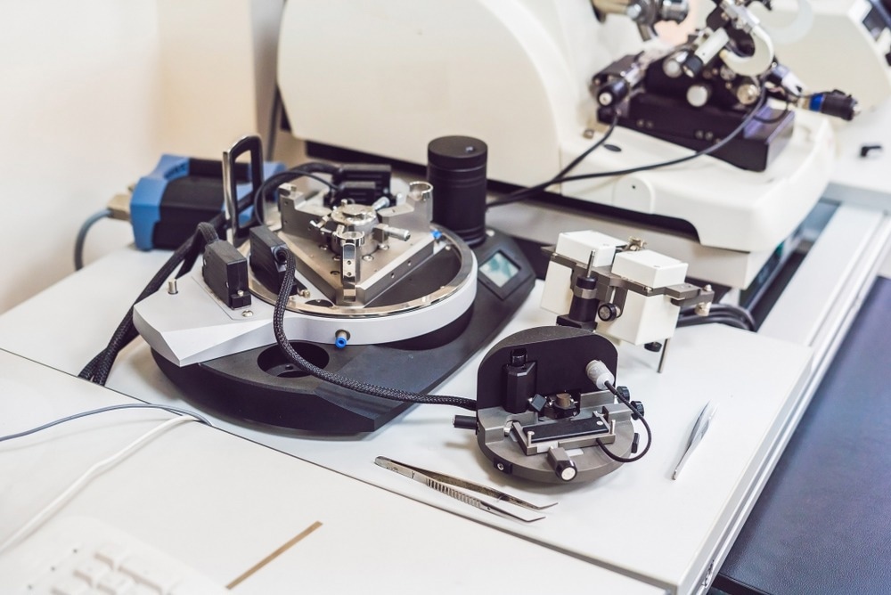
The prepared molybdenene sheets were glued onto silicon chips to fabricate cantilevers for AFM analysis. Thus, the fabricated cantilevers offered two possible orientations because of a layered material with in-plane covalent bonding and interplanar van der Waals interactions.
The layers in the first orientation were stacked one above the other, with flexibility reduced along the lateral direction and dominant across the vertical direction. This type of cantilever is suitable for high-resolution imaging in the dynamic force mode because it reduces noise in the lateral direction.
On the other hand, in the second orientation, flexibility is restricted in the vertical direction, where the layers are stacked laterally, reducing the noise associated with vertical deflection. This type of cantilever can image versatile materials, such as smooth 2D surfaces, soft biomolecules, and hard silicon structures.
The cantilever tip was prepared by carefully bending its sharp end. The manufactured cantilever demonstrated close agreement with commercially available cantilevers, with a resonance frequency of approximately 135 kHz and a Q factor of approximately 160.
The manufactured cantilevers are intrinsically metallic and highly reflective, which improves the sensitivity of laser-based photodiode detectors to deflections. Fabricated cantilevers also have an advantage over commercially available metal-coated silicon cantilevers, which frequently fail because of metal coating delamination during imaging.

Image Credit: Elizaveta Galitckaia/Shutterstock.com
Molybdenene-based 2D–2D Hybrids
Mo hybridized with BN showed both peaks in the Raman spectra. The Mo layer showed structural reconfiguration owing to the robust electrostatic interlayer coupling between the two heterolayers. This type of atomic structure evolution/reconfiguration is crucial in 2D hybrid materials.
The high-resolution tunneling electron microscope (HRTEM) image of the Mo-BN heterolayer revealed criss-cross patterns, and the electron diffraction pattern showed the area’s square crystal symmetry. HRTEM images of this hybrid also revealed an atomic sheet comprising Mo atoms above another atomic sheet, constituting B and N atoms, which are smaller than Mo atoms.
Similarly, Raman spectroscopy of the M–MoS2 hybrid showed Mo and MoS2 sheets. The elemental profile and TEM images revealed two different statistically distributed structures: stripe patterns of atoms in the M–MoS2 system and hexagonal symmetry in the crystal structure, unveiled using HRTEM.
Conclusion
Overall, the fabrication of molybdenene represents a significant breakthrough in realizing 2D Dirac-like materials. The fascinating structure of molybdenene containing only Mo atoms is a remarkable achievement and paves the way for constructing more reliable electronic devices.
Contaminant-free Dirac materials such as molybdenene are promising candidates for enhancing the electronic mobility, which is crucial for future technological leaps. Hybridizing molybdenene with 2D h-BN and MoS2 has opened avenues toward tailoring the optical and electronic properties, which are crucial for diverse applications. Thus, exploring molybdenene highlights the pivotal role of 2D Dirac-like materials in advancing photonics and electronics.
The characterization of molybdenene revealed its interesting structural characteristics, including its metallic nature, millimeter-long whiskers with loosely linked sheets, and remarkable electrical conductivity. Leveraging these properties of molybdenene enables the fabrication of microscope cantilevers with several orientations, ideal for a range of imaging requirements, such as noise reduction during vertical deflection or high-resolution dynamic force mode imaging.
Molybdenene’s journey epitomized a fascinating fusion of innovation and collaboration in material science, opening new avenues in the realm of 2D materials and their hybrids. As research progresses, harnessing the unique properties of molybdenene holds promise for diverse technological frontiers, from catalysis to advanced imaging.
See More: Customizing Graphene with Doping: How and Why?
References and Further Reading
Sahu, T. K . et al. (2023). Microwave synthesis of molybdenene from MoS2. Nature Nanotechnology, pp. 1-9. doi.org/10.1038/s41565-023-01484-2
Jülich, F. (2023). Beyond Graphene: A New ‘Metallic’ 2D Material – Molybdenene. [online] SciTechDaily. Available at: https://scitechdaily.com/beyond-graphene-a-new-metallic-2d-material-molybdenene/
www.chemeurope.com. (n.d.). Molybdenene – the ‘Metallic’ Relative of Graphene. [online] Available at: https://www.chemeurope.com/en/news/1181628/molybdenene-the-metallic-relative-of-graphene.html


