


By
Artist’s impression of the chip surface, showing the on-chip light interferometer used to sense the presence of lead. The lead binding process to the crown ether is shown in the inset. Credit: Jia Xu Brian Sia
A new chip-scale device could provide sensitive detection of lead levels in drinking water, whose toxicity affects 240 million people worldwide.
Engineers at MIT and collaborators have developed a compact, inexpensive technology to detect and measure lead in water. This new system uses a photonic chip and crown ethers to capture lead ions, providing accurate, near-instant results with just a droplet of water.
Engineers at MIT, Nanyang Technological University, and several companies have developed a compact and inexpensive technology for detecting and measuring lead concentrations in water, potentially enabling a significant advance in tackling this persistent global health issue.
The World Health Organization estimates that 240 million people worldwide are exposed to drinking water that contains unsafe amounts of toxic lead, which can affect brain development in children, cause birth defects, and produce a variety of neurological, cardiac, and other damaging effects. In the United States alone, an estimated 10 million households still get drinking water delivered through lead pipes.
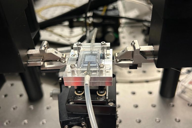
Testing setup of the photonic chip sensor, including microfluidic chamber to transport analyte solutions and optical fibers on the sides to measure the photonic response of the chip. Credit: Courtesy of the researchers
“It’s an unaddressed public health crisis that leads to over 1 million deaths annually,” says Jia Xu Brian Sia, an MIT postdoc and the senior author of the paper describing the new technology.
However, testing for lead in water requires expensive, cumbersome equipment and typically requires days to get results. Or, it uses simple test strips that simply reveal a yes-or-no answer about the presence of lead but no information about its concentration. Current EPA regulations require drinking water to contain no more than 15 parts per billion of lead, a concentration so low it is difficult to detect.
Innovative Photonic Chip Technology
The new system, which could be ready for commercial deployment within two or three years, could detect lead concentrations as low as 1 part per billion, with high accuracy, using a simple chip-based detector housed in a handheld device. The technology gives nearly instant quantitative measurements and requires just a droplet of water.
The findings are described in a paper published on May 14 in the journal Nature Communications, by Sia, MIT graduate student and lead author Luigi Ranno, Professor Juejun Hu, and 12 others at MIT and other institutions in academia and industry.
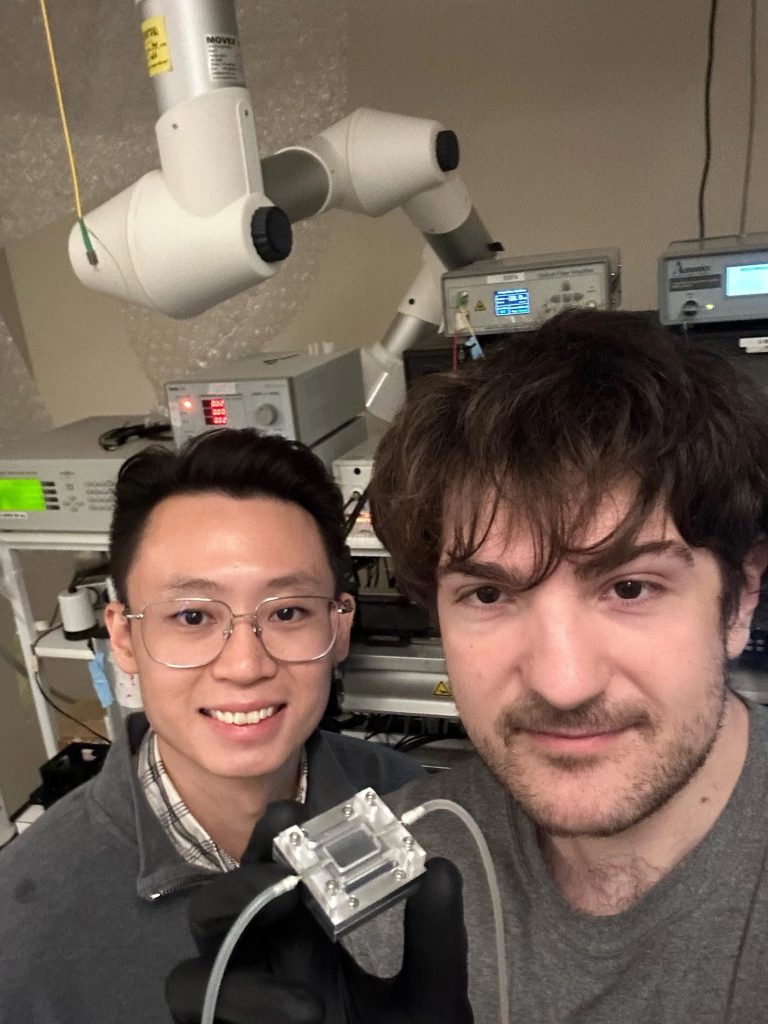
Jia Xu Brian Sia (left) and Luigi Ranno (right) showcasing the fully packaged sensor chip and microfluidic chamber. Credit: Courtesy of the researchers
The team set out to find a simple detection method based on the use of photonic chips, which use light to perform measurements. The challenging part was finding a way to attach to the photonic chip surface certain ring-shaped molecules known as crown ethers, which can capture specific ions such as lead. After years of effort, they were able to achieve that attachment via a chemical process known as Fischer esterification. “That is one of the essential breakthroughs we have made in this technology,” Sia says.
In testing the new chip, the researchers showed that it can detect lead in water at concentrations as low as one part per billion. At much higher concentrations, which may be relevant for testing environmental contamination such as mine tailings, the accuracy is within 4 percent.
Versatility and Practical Applications
The device works in water with varying levels of acidity, ranging from pH values of 6 to 8, “which covers most environmental samples,” Sia says. They have tested the device with seawater as well as tap water, and verified the accuracy of the measurements.
In order to achieve such levels of accuracy, current testing requires a device called an inductive coupled plasma mass spectrometer. “These setups can be big and expensive,” Sia says. The sample processing can take days and requires experienced technical personnel.
While the new chip system they developed is “the core part of the innovation,” Ranno says, further work will be needed to develop this into an integrated, handheld device for practical use. “For making an actual product, you would need to package it into a usable form factor,” he explains. This would involve having a small chip-based laser coupled to the photonic chip. “It’s a matter of mechanical design, some optical design, some chemistry, and figuring out the supply chain,” he says. While that takes time, he says, the underlying concepts are straightforward.
The system can be adapted to detect other similar contaminants in water, including cadmium, copper, lithium, barium, cesium, and radium, Ranno says. The device could be used with simple cartridges that can be swapped out to detect different elements, each using slightly different crown ethers that can bind to a specific ion.
Impact on Global Health
“There’s this problem that people don’t measure their water enough, especially in the developing countries,” Ranno says. “And that’s because they need to collect the water, prepare the sample, and bring it to these huge instruments that are extremely expensive.” Instead, “having this handheld device, something compact that even untrained personnel can just bring to the source for on-site monitoring, at low costs,” could make regular, ongoing widespread testing feasible.
Hu, who is the John F. Elliott Professor of Materials Science and Engineering, says, “I’m hoping this will be quickly implemented, so we can benefit human society. This is a good example of a technology coming from a lab innovation where it may actually make a very tangible impact on society, which is of course very fulfilling.”
“If this study can be extended to simultaneous detection of multiple metal elements, especially the presently concerning radioactive elements, its potential would be immense,” says Hou Wang, an associate professor of environmental science and engineering at Hunan University in China, who was not associated with this work.
Wang adds, “This research has engineered a sensor capable of instantaneously detecting lead concentration in water. This can be utilized in real-time to monitor the lead pollution concentration in wastewater discharged from industries such as battery manufacturing and lead smelting, facilitating the establishment of industrial wastewater monitoring systems. I think the innovative aspects and developmental potential of this research are quite commendable.”
Wang Qian, a principal research scientist at the Institute of Materials Research in Singapore, who also was not affiliated with this work, says, “The ability for the pervasive, portable, and quantitative detection of lead has proved to be challenging primarily due to cost concerns. This work demonstrates the potential to do so in a highly integrated form factor and is compatible with large-scale, low-cost manufacturing.”
Reference: “Crown ether decorated silicon photonics for safeguarding against lead poisoning” by Luigi Ranno, Yong Zen Tan, Chi Siang Ong, Xin Guo, Khong Nee Koo, Xiang Li, Wanjun Wang, Samuel Serna, Chongyang Liu, Rusli, Callum G. Littlejohns, Graham T. Reed, Juejun Hu, Hong Wang and Jia Xu Brian Sia, 14 May 2024, Nature Communications.
DOI: 10.1038/s41467-024-47938-6
The team included researchers at MIT, at Nanyang Technological University and Temasek Laboratories in Singapore, at the University of Southampton in the U.K., and at companies Fingate Technologies, in Singapore, and Vulcan Photonics, headquartered in Malaysia. The work used facilities at MIT.nano, the Harvard University Center for Nanoscale Systems, NTU’s Center for Micro- and Nano-Electronics, and the Nanyang Nanofabrication Center.
