


Assemblies of quantum dots tend to be highly disordered, but when the facets of these tiny semiconducting structures are lined up like soldiers on parade, something strange happens: the dots become very good at conducting electricity. This is the finding of researchers at the RIKEN Center for Emergent Matter Science in Japan, who say that these ordered, quasi-two-dimensional “superlattices” of quantum dots could make it possible to develop faster and more efficient electronics.
Quantum dots are semiconductor structures that confine electrons in all three spatial dimensions. This confinement means that quantum dots behave in some ways like single quantum particles even though they contain thousands of atoms and measure up to 50 nm across. Thanks to their particle-like properties, quantum dots have found use in many optoelectronics applications, including solar cells, biological imaging systems and electronic displays.
There is a snag, however. The general disorderliness of quantum dot assemblies means that charge carriers do not flow efficiently through them. This makes their electrical conductivity poor, and standard techniques for introducing order have not helped much. “Although the order of the assemblies can be improved, we found that it is not enough,” says Satria Zulkarnaen Bisri, who led the RIKEN study and is now an associate professor at the Tokyo University of Agriculture and Technology.
A fresh look at quantum dots
Bisri explains that to improve quantum dots’ conductivity, we need to look at them in a different way – not as spherical objects, as is currently the case, but as chunks of matter with a suite of unique crystallographic properties inherited from their compound crystal structure. “Orientation uniformity of the quantum dots is also important,” he says. “Understanding this enabled us to formulate a way to control the assembly of the quantum dots by tuning the interaction between facets of neighbouring quantum dots.”
The researchers made their quantum dot assemblies, or superlattices, by creating what is known as a Langmuir film. Bisri describes this process as a bit like drizzling oil on the surface of water and letting it spread into a very thin layer. In their experiment, the “oil” is the quantum dots, while the “water” is a solvent that helps the dots connect to each other selectively, via certain facets, to form an ordered monolayer, or superlattice.
“The good properties of this monolayer superlattice are that the large-scale order and the coherent orientation of the quantum dot building blocks minimize energetic disorders throughout the assembly,” Bisri tells Physics World. “This allows for more precise control over the electronic properties of the dots.”
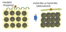
The RIKEN researchers found that they could make their system up to a million times more conductive than assemblies of quantum dots that were not connected epitaxially in this way. Bisri explains that this increase in conductivity is associated with an increase in the doping level of charge carriers in the system. At this higher doping, charge transport from one quantum dot to another is no longer governed by a hopping transport process (as occurs in an insulator), but by a delocalized transport mechanism through electronic minibands – “just as what would happen in a metallic material,” Bisri says.
Faster and more efficient electronic devices
High conductivity and metallic behaviour in semiconducting colloidal quantum dots could bring significant advantages for electronic devices, making it possible to develop faster and more efficient transistors, solar cell, thermoelectrics, displays and sensors (including photodetectors), Bisri adds. The materials could also be used to investigate fundamental physical phenomena such as strongly correlated and topological states.
The researchers now plan to study other quantum dot compounds. “We would also like to achieve similar or even better metallic behaviour using other means besides electrical field-induced doping,” Bisri reveals.
They detail their present work in Nature Communications.
