In electronic technologies, key material properties change in response to stimuli like voltage or current. Scientists aim to understand these changes in terms of the material’s structure at the nanoscale (a few atoms) and microscale (the thickness of a piece of paper). Often neglected is the realm between the mesoscale—spanning 10 billionths to 1 millionth of a meter.
Scientists at the U.S. Department of Energy’s (DOE) Argonne National Laboratory, in collaboration with Rice University and DOE’s Lawrence Berkeley National Laboratory, have made significant strides in understanding the mesoscale properties of a ferroelectric material under an electric field. The research is published in the journal Science.
This breakthrough holds potential for advances in computer memory, lasers for scientific instruments and sensors for ultraprecise measurements.
The ferroelectric material is an oxide containing a complex mixture of lead, magnesium, niobium and titanium. Scientists refer to this material as a relaxor ferroelectric. It is characterized by tiny pairs of positive and negative charges, or dipoles, that group into clusters called “polar nanodomains.”
Under an electric field, these dipoles align in the same direction, causing the material to change shape, or strain. Similarly, applying a strain can alter the dipole direction, creating an electric field.
“If you analyze a material at the nanoscale, you only learn about the average atomic structure within an ultrasmall region,” said Yue Cao, an Argonne physicist. “But materials are not necessarily uniform and do not respond in the same way to an electric field in all parts. This is where the mesoscale can paint a more complete picture bridging the nano- to microscale.”
A fully functional device based on a relaxor ferroelectric was produced by professor Lane Martin’s group at Rice University to test the material under operating conditions. Its main component is a thin film (55 nanometers) of the relaxor ferroelectric sandwiched between nanoscale layers that serve as electrodes to apply a voltage and generate an electric field.
Using beamlines in sectors 26-ID and 33-ID of Argonne’s Advanced Photon Source (APS), Argonne team members mapped the mesoscale structures within the relaxor.
Key to the success of this experiment was a specialized capability called coherent X-ray nanodiffraction, available through the Hard X-ray Nanoprobe (Beamline 26-ID) operated by the Center for Nanoscale Materials at Argonne and the APS. Both are DOE Office of Science user facilities.
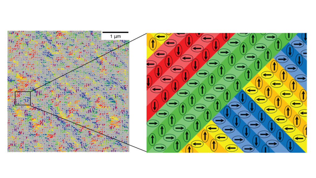
The results show that, under an electric field, the nanodomains self-assemble into mesoscale structures consisting of dipoles that align in a complex tile-like pattern. The team identified the strain locations along the borders of this pattern and the regions responding more strongly to the electric field.
“These submicroscale structures represent a new form of nanodomain self-assembly not known previously,” noted John Mitchell, an Argonne Distinguished Fellow. “Amazingly, we could trace their origin all the way back down to underlying nanoscale atomic motions…”
“Our insights into the mesoscale structures provide a new approach to the design of smaller electromechanical devices that work in ways not thought possible,” Martin said.
“The brighter and more coherent X-ray beams now possible with the recent APS upgrade will allow us to continue to improve our device,” said Hao Zheng, the lead author of the research and a beamline scientist at the APS.
“We can then assess whether the device has application for energy-efficient microelectronics, such as neuromorphic computing modeled on the human brain.” Low-power microelectronics are essential for addressing the ever-growing power demands from electronic devices around the world, including cell phones, desktop computers and supercomputers.


