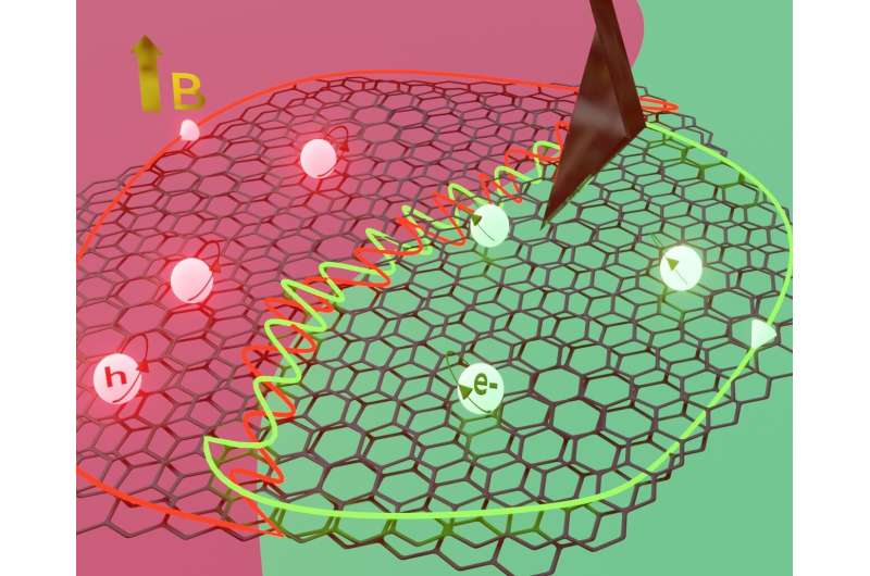
Recent advances in the development of devices made of 2D materials are paving the way for new technological capabilities, especially in the field of quantum technology. So far, however, little research has been carried out into energy losses in strongly interacting systems.
With this in mind, the team led by Professor Ernst Meyer from the Department of Physics at the University of Basel used an atomic force microscope in pendulum mode to investigate a graphene device in greater detail. For this, the researchers utilized a two-layer graphene, fabricated by colleagues at LMU Munich, in which the two layers were twisted by 1.08°.
When stacked and twisted relative to one another, the two layers of graphene produce “moiré” superstructures, and the material acquires new properties. For example, when the two layers are twisted by the so-called magic angle of 1.08°, graphene becomes a superconductor at very low temperatures, conducting electricity with almost no energy dissipation.
Fine-tuning the properties
Using atomic force microscopy (AFM) measurements, Dr. Alexina Ollier has now been able to prove that the twist angle of the atomic graphene layers was uniform across the entire layer, at about 1.06°. She was also able to measure how the current-conducting properties of the graphene layer can be changed and adjusted as a function of the charge applied to the device.
Depending on the “charging” of the individual graphene cells with electrons, the material behaved as an insulator or a semiconductor. The relatively high temperature of 5 Kelvin (-268.15°C) during the measurements meant that the researchers did not achieve superconductivity in the graphene, as this phenomenon—current conduction with no energy dissipation—only occurs at a much lower temperature of 1.7 Kelvin.
“We were able, however, not only to modify and measure the current-conducting properties of the device,” explains Ollier, first author of the study now published in Communications Physics, “but also to impart magnetic properties to the graphene—which, of course, consists of nothing but carbon atoms.”
“It is an achievement that we’re able to image tiny graphene flakes in electrical components, change their electrical and magnetic properties, and measure them precisely,” says Meyer regarding the work, which formed part of a doctoral thesis at the SNI Ph.D. School. “In the future, this method will also help us to determine the energy loss of various two-dimensional components in the event of strong interactions.”


