


Conductive nanowires have recently undergone extensive investigation due to their potential application as transparent conducting electrodes in flexible electronics, organic light-emitting diodes OLEDs, wearable biosensors (wearable electronics), and solar cells.1-3
Image Credit: Harrick Plasma
While indium tin oxide (ITO) is commonly employed as a transparent conducting electrode in the manufacture of current devices, it is not a suitable material for flexible electronics due to its relative brittleness, higher production cost (typically through vacuum deposition), and significant challenges in obtaining indium.
As a result of their nanometer scale, nanowires possess intrinsic optical transparency and mechanical flexibility, meeting most criteria for electrodes in flexible electronics. These criteria include high electrical conductivity, high optical transmission, flexibility, and structural stability to endure repeated and continuous deformation cycles.
Researchers have recently explored different materials and methods for fabricating nanowires. Silver and gold nanowires (AgNW, AuNW) are considered suitable alternatives to ITO because they can be deposited using simple and cost-effective techniques like spin, dip, or spray coating from solution; drop casting; or self-assembly.
Researchers are also focusing on fabricating nanowires that can be precisely patterned, cover a large surface area with relative smoothness, and can be scaled for mass production.
Having clean, hydrophilic surfaces is crucial for fabricating nanowires from solution. This is important so that the solution can be readily wet and uniformly distributed across the surface with strong adhesion. This is essential for optimal device performance.
Plasma treatment eliminates residual organic contamination and presents oxygen-containing polar functional groups (hydroxyl, carbonyl, carboxyl) to increase the hydrophilicity of the surface.
This article explores the application of plasma treatment to facilitate nanowire fabrication and enhance electrical properties for optimal device performance.
Fabricating Nanowires
To prepare substrate surfaces for nanowire fabrication, plasma treatment is frequently conducted before the deposition step. Plasma cleaning makes surfaces hydrophilic and encourages uniform distribution of the nanowire solution onto the surface.
In certain instances, an intermediate layer may be applied on the plasma-treated substrate to enhance and facilitate the adhesion of the nanowire to the substrate. Plasma-treated and hydrophilic surfaces have also been utilized to generate patterned nanowire networks (shown in Figure 1).
Chen et al. applied AgNWs to flexible polydimethylsiloxane PDMS substrates. Since PDMS is inherently hydrophobic, air plasma was initially used on PDMS through a patterned mask.
The plasma transformed the exposed PDMS into a patterned hydrophilic/hydrophobic surface, defining the areas for nanowire deposition areas. The solution-cast nanowires adhered to the hydrophilic regions but did not adhere to the untreated, hydrophobic areas.
In another example, Gao et al. employed O2 plasma to make PDMS hydrophilic before stretching, resulting in well-defined, periodic wrinkles. The periodicity and height of the wrinkle were controlled by the magnitude of the applied strain.
The wrinkled PDMS functioned as a periodic template and was subsequently spray-coated with a dispersion of AgNWs to create a patterned nanowire layer.
Following the patterning process, the nanowires can be embedded into a flexible optical coating (such as Ecoflex, UV curable polyurethane optical adhesive, and PDMS) to create a nanowire/polymer composite.
This resulting nanowire composite is optically transparent, flexible, and stretchable while maintaining a relatively smooth and continuous wire network with repeated mechanical strain cycles. All these properties are critical for applications such as flexible/wearable electronics.
The patterned AgNW composite prepared by Chen et al. demonstrated optical and electrical properties roughly similar to that of ITO. It had an average sheet resistance RS of approximately 15 Ω/sq. and an optical transmittance of about 85 % at 550 nm. For Gao et al., the patterned AgNWs exhibited RS of 18 Ω/sq. and an optical transmittance of 78 %.
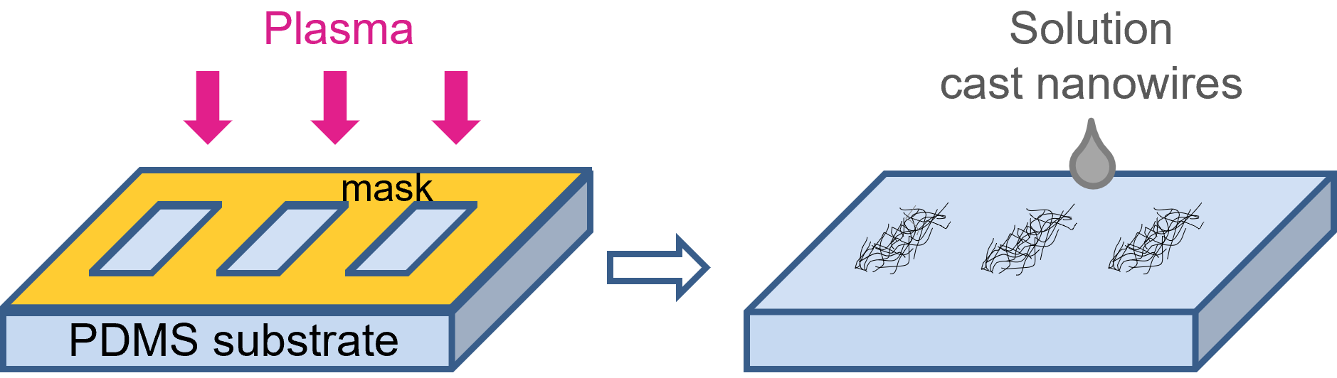
Figure 1. An example of patterning nanowires on PDMS substrate, an inherently hydrophobic material. Plasma renders the exposed surfaces hydrophilic. Nanowire solution coats the hydrophilic areas to create a patterned nanowire layer. Image Credit: Harrick Plasma
Improving Nanowire Electrical Properties
Plasma treatment has been used to enhance nanowire electrical properties and produce highly conductive electrodes. In the study by Li et al., Ar plasma was applied to AgNWs that were spin-coated from the solution. This removes residual polyvinylpyrrolidone PVP surfactant (from the deposition process).
Plasma treatment fused neighboring AgNWs to enhance electrical contact between the nanowires.
Similarly, Gong et al. employed Ar plasma on self-assembled AuNWs to eliminate surplus oleylamine OA ligand (from the self-assembly process) and promote intimate contact at the nanowire junctions, consequently reducing electrical resistance.
According to Li et al’s study research, the resulting AgNW sheet resistance with different plasma treatment durations indicated a decrease from at least 25 Ω/sq. (as deposited) to 7-8 Ω/sq. with up to 15 minutes of plasma (shown in Figure 2).
Prolonged plasma exposure, however, resulted in an increased sheet resistance. SEM images revealed breaks and discontinuity along the length of the nanowires, signifying melting and damage to AgNW with extreme plasma exposure.
Li et al. discovered that adjusting treatment time was critical, and they found that 15-minute plasma produced optimal nanowire performance. This resulted in a sheet resistance of approximately 7 Ω/sq. while maintaining 78 % optical transmittance at 550 nm, and an electron work function of 5.84 eV.
For comparison, traditional heating of AgNWs (150 °C for 15 minutes) produced a higher sheet resistance of 20-25 Ω/sq., approximately 72 % optical transmittance at 550 nm, and a work function of 5.5 eV. Other researchers have indicated that longer thermal annealing times (up to 200 minutes) may be needed to reduce AgNW sheet resistance.4
Li et al.’s work showcases that plasma treatment is an important step in enhancing the electrical properties of AgNW deposited from solution, leading to optimal device performance.
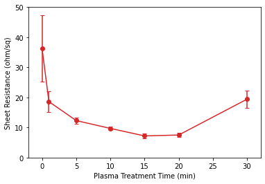
Figure 2. Sheet resistance RS of solution cast AgNW with Ar plasma treatment. Ar plasma removed residual organic PVP (from coating process) and enhanced contact between adjacent nanowires. Data from Li J, Tao Y, Chen S, Li H, Chen P, Wei M-z, Wang H, Li K, Mazzeo M, and Duan Y. “A flexible plasma-treated silver-nanowire electrode for organic light-emitting devices”. Sci. Rep. (2017) 7(1): 16468. 10.1038/s41598-017-16721-7
References and Further Reading
Fabricating Nanowires: Articles by Harrick Plasma Users
- An T, Anaya DV, Gong S, Yap LW, Lin F, Wang R, Yuce MR and Cheng W. “Self-powered gold nanowire tattoo triboelectric sensors for soft wearable human-machine interface”. Nano Energy (2020) 77: 105295. 10.1016/j.nanoen.2020.105295
- An T, Gong S, Ling Y, Dong D, Zhao Y, and Cheng W. “Dynamically functioning and highly stretchable epidermal supercapacitor based on vertically aligned gold nanowire skins”, EcoMat. (2020) 2: e12022. 10.1002/eom2.12022
- An T, Ling Y, Gong S, Zhu B, Zhao Y, Dong D, Yap L, Wang Y, and Cheng W. “A Wearable Second Skin‐Like Multifunctional Supercapacitor with Vertical Gold Nanowires and Electrochromic Polyaniline”. Adv. Mater. Technol. (2019) 4: 1800473. 10.1002/admt.201800473
- Ji B, Zhou Q, Wu J, Gao Y, Wen W and Zhou B. “Synergistic Optimization towards the Sensitivity and Linearity of Flexible Pressure Sensor via Double Conductive Layer and Porous Micro-dome Array”. ACS Appl. Mater. Interfaces (2020) 12: 31021-31035. 10.1021/acsami.0c08910
- Ji B, Mao Y, Zhou Q, Zhou J, Chen G, Gao Y, Tian Y, Wen W, and Zhou B. “Facile Preparation of Hybrid Structure Based on Mesodome and Micropillar Arrays as Flexible Electronic Skin with Tunable Sensitivity and Detection Range”. ACS Appl. Mater. Interfaces (2019) 11: 28060-28071. 10.1021/acsami.9b08419
- Gao Z, Yiu C, Liu Y, Li D, Mei L, Zeng Z, and Yu X. “Stretchable transparent conductive elastomers for skin-integrated electronics”. J. Mater. Chem. C (2020) 8: 15105-15111. 10.1039/D0TC02913K
- Chen Y, Carmichael R, and Carmicharel T. “Patterned, Flexible, and Stretchable Silver Nanowire/Polymer Composite Films as Transparent Conductive Electrodes”. ACS Appl. Mater. Interfaces (2019) 11: 31210-31219. 10.1021/acsami.9b11149
Improving Nanowire Electrical Properties: Articles by Harrick Plasma Users
- Li J, Tao Y, Chen S, Li H, Chen P, Wei M-z, Wang H, Li K, Mazzeo M, and Duan Y. “A flexible plasma-treated silver-nanowire electrode for organic light-emitting devices”. Sci. Rep. (2017) 7(1): 16468. 10.1038/s41598-017-16721-7
- Gong S, Zhao Y, Shi Q, Wang Y, Yap LW, and Cheng W. “Self-assembled Ultrathin Gold Nanowires as Highly Transparent, Conductive and Stretchable Supercapacitor”. Electroanalysis (2016) 28(6): 1298-1304. 10.1002/elan.201600081
- Gong S, Zhao Y, Yap LW, Shi Q, Wang Y, Bay JAPB, Lai DTH, Uddin H, and Cheng W. “Fabrication of Highly Transparent and Flexible NanoMesh Electrode via Self-assembly of Ultrathin Gold Nanowires”. Adv. Electron. Mater. (2016) 2: 1600121. 10.1002/aelm.201600121
Supplemental References (Do Not Report Using Harrick Plasma Cleaners)
- Huang Q and Zhu Y. “Patterning of Metal Nanowire Networks: Methods and Applications.” ACS Appl. Mater. Interfaces (2021) 13: 60736-60762.
- Zhang R and Engholm, M. “Recent Progress on the Fabrication and Properties of Silver Nanowire-Based Transparent Electrodes.” Nanomaterials (2018) 8: 628.
- Sannicolo T, Lagrange M, Cabos A, Celle C, Simonato J-P and Bellet D. “Metallic Nanowire-Based Transparent Electrodes for Next Generation Flexible Devices: a Review.” Small (2016) 12(44): 6052–6075.
- Coskun S, Ates ES, Unalan HE. “Optimization of silver nanowire networks for polymer light emitting diode electrodes.” Nanotechnology (2013) 24: 125202.
This information has been sourced, reviewed, and adapted from materials provided by Harrick Plasma.
For more information on this source, please visit Harrick Plasma.
