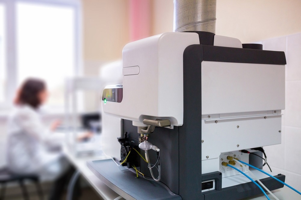
Atomic emission spectroscopy (AES) is an analytical technique that analyzes the electromagnetic radiation emitted from a sample to identify and quantify the different species within it.
Image Credit: Sodel Vladyslav/Shutterstock.com
AES typically involves creating plasma from the sample. Several inductively coupled plasma (ICP) techniques can be used either with standard mass spectrometry (ICP-MS)—a popular method for trace element analysis in many industries—or with optical emission spectroscopy (OES) and AES detection methods.1
Principles of Atomic Emission Spectroscopy
Transitions between different electronic energy levels in elements occur at unique energies and intensities, giving each element a distinctive emission spectrum.
When the energy of an incident photon matches the energy difference between two electronic energy levels in an atom, the atom absorbs the photon, promoting an electron to a higher energy level and creating an excited state.
Most excited states are metastable and have very short lifetimes, often less than a billionth of a second. An isolated atom, with no environmental interactions, can only release the excess energy from the absorbed photon by emitting another photon. Due to energy conservation laws, the emitted photon’s energy equals the energy difference between the two involved energy levels.
This emitted photon is detected in AES and used to identify the element. Even the simplest element, hydrogen, has many possible electronic energy levels, forming a converging series as energy increases. Consequently, the energy spacing between subsequent electronic energy levels becomes smaller at higher energies.
An element can absorb photons of many different energies due to multiple possible transitions between different energy levels.
In atomic spectra, absorption and emission lines are very sharp because the associated transitions have narrow line widths, and the absorption and emission spectra are typically inverses of each other.
The patterns of spectral lines are analyzed for element identification, with the Fraunhofer lines in the sun’s absorption spectrum being a well-known example.2 These lines appear due to elements such as hydrogen and sodium.
Instrumentation and Set-Up
Plasmas are popular in AES measurements because most elements are in their electronic ground state under standard laboratory conditions, requiring high-energy photons to excite many transitions.
Creating a plasma with a light source generates highly excited states, allowing more of the emission spectrum to be observed and enabling multiple elements to be excited simultaneously. While narrow-band laser sources could selectively excite specific transitions, only a subset of transitions could be measured at a time.
For some experiments, a flame may suffice for sample combustion, but sources like an arc or spark are often used to create plasma.3 ICP sources use radio frequencies and a ‘carrier gas’ to create the plasma.4 The tunable radio frequencies create a high-temperature plasma that interacts with the sample, with ICP methods being popular due to their controllable plasma conditions.
The detection method and choice of monochromator are also important when developing AES instrumentation.5 Monochromators allow a selected range of wavelengths to pass through, which is useful for controlling both excitation and detection conditions.
Since plasmas provide a continuous emission background, AES can reduce interference from stray light or allow analysis after exciting only a subset of the elements for more precise analysis.
Detectors can be imaging-type CCD detectors or single-wavelength photomultiplier tubes (PMTs). CCDs are advantageous because they can detect multiple emission lines simultaneously without scanning the detection wavelength using a monochromator. Still, they can be more expensive and potentially less sensitive than some PMTs.
Sample Preparation
AES involves various sample preparation techniques depending on the sample’s state (for instance, solid or liquid) and the elements to be detected.
Ideally, the matrix used should contain the same elements as the sample to avoid measurement interference. Some samples may need treatment to remove excess organic content or filtration to reduce matrix or background signals in the AES measurement.
Application of AES in Nanoscience
AES, particularly ICP-AES, is commonly used for elemental analysis in nanoscience, especially for analyzing the composition of nanoparticles. Nanotoxicity analysis, particularly for environmental samples, is another application where AES’s high sensitivity to trace elements is advantageous.6
Analysis of AES data often involves comparing recorded spectra to spectral databases. For atomic species with well-known transition energies and intensities, it is possible to model and predict spectra for different combinations.
Highly charged and radical species may prove more challenging, but varying excitation and detection conditions can help identify the species present and the transitions observed in the final spectra.
More from AZoNano: Are There Alternatives to Semiconductor Chips?
References and Further Reading
- Yeung, V., Miller, DD., Rutzke, MA. (2017). Atomic absorption spectroscopy, atomic emission spectroscopy, and inductively coupled plasma-mass spectrometry. Food Analysis. doi.org/10.1007/978-3-319-45776-5_9
- Paldus, BA., Zare, RN. (1999). Historical Overview of Spectral Studies : From Sunlight to Lasers. ACS Symposium Series. doi.org/10.1021/bk-1999-0720.ch001
- Bings, NH., Bogaerts, A., Broekaert, AC. (2010). Atomic Spectroscopy : A Review. Analytical Chemistry. doi.org/10.1021/ac1010469
- Terentev, TN., Shemakhin, AY., Samsonova, ES., Zheltukhin, VS. (2022). Frequency dependencies of the characteristics of an inductively coupled radiofrequency discharge. Plasma Sources Science and Technology. doi.org/ 10.1088/1361-6595/ac8dba
- Smith, CMM., Taylor, RN. (2018). Atomic spectroscopy update: review of advances in atomic spectrometry and related techniques. J. Anal. At. Spectrom. doi.org/10.1039/c8ja90012d
- Liu, Y., Zhu, S., Gu, Z., Chen, C., Zhao, Y. (2022). Particuology Toxicity of manufactured nanomaterials. Particuology. doi.org/10.1016/j.partic.2021.11.007


