Close Menu
  • News
  • Medical
  • Technology
  • Nanomaterials
  • Research
  • Blog
    • Nasiol.com
  • Contact
    • Tech7685@gmail.com
What's Hot

A new molecular model of bilayer graphene with higher semiconducting properties

May 31, 2025

5 Nanomaterial Innovations That Didn’t Deliver (Yet)

May 30, 2025

Scientists identify new 2D copper boride material with unique atomic structure

May 30, 2025
Facebook X (Twitter) Instagram
Nanotech – Nanomaterials | Medical | Research | News Stories Updated Daily Nanotech – Nanomaterials | Medical | Research | News Stories Updated Daily
  • News
  • Medical
  • Technology
  • Nanomaterials
  • Research
  • Blog
    • Nasiol.com
  • Contact
    • Tech7685@gmail.com
Facebook X (Twitter) Instagram
Nanotech – Nanomaterials | Medical | Research | News Stories Updated Daily Nanotech – Nanomaterials | Medical | Research | News Stories Updated Daily
Home»News»Graphene technique improves ultrathin film manufacturing for flexible electronics
News

Graphene technique improves ultrathin film manufacturing for flexible electronics

January 16, 2025No Comments3 Mins Read
Facebook Twitter Pinterest Telegram LinkedIn Tumblr WhatsApp Email
Graphene technique improves ultrathin film manufacturing for flexible electronics
Share
Facebook Twitter LinkedIn Pinterest Telegram Email
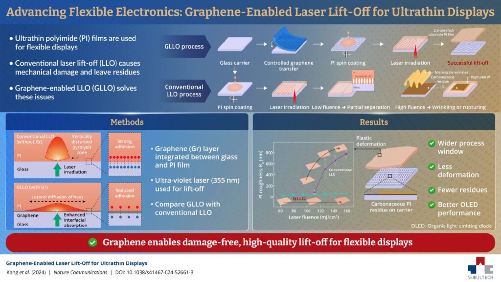
The graphene layer improves ultra-violet light absorption, evenly distributes heat, and reduces adhesion, resulting in flawless and flexible displays. This innovation brings us closer to next-generation wearable electronics and stretchable technologies. Credit: Prof. Sumin Kang, SEOULTECH, South Korea

As the demand for thinner, lighter, and more flexible electronic devices grows, the need for advanced manufacturing processes has become critical. Polyimide (PI) films are widely used in these applications due to their excellent thermal stability and mechanical flexibility. They are crucial for emerging technologies like rollable displays, wearable sensors, and implantable photonic devices.

However, when the thickness of these films is reduced below 5 μm, traditional laser lift-off (LLO) techniques often fail. Mechanical deformation, wrinkling, and leftover residues frequently compromise the quality and functionality of ultrathin devices, making the process inefficient and costly.

In this view, researchers turned to graphene, a nanomaterial known for its exceptional thermal and mechanical properties. A research team from Seoul National University of Science and Technology, led by Professor Sumin Kang, has designed a novel technique to overcome the challenges with the LLO process.

Their innovative graphene-enabled enhanced laser lift-off (GLLO) method ensures ultrathin displays can be separated smoothly and without damage—making them perfect for wearable applications. Their study was published in the journal Nature Communications on September 27, 2024.

In this study, they have introduced a novel GLLO process that integrates a layer of chemical vapor deposition-grown graphene between the PI film and its glass carrier.

“Graphene’s unique properties, such as its ability to absorb ultra-violet (UV) light and distribute heat laterally, enable us to lift off thin substrates cleanly, without leaving wrinkles or residues,” says Prof. Kang.

Graphene breakthrough: SEOULTECH's laser technology unveils damage-free ultrathin flexible displays
Application of the GLLO method to ultrathin organic light-emitting diode (OLED) devices. Credit: Nature Communications (2024). DOI: 10.1038/s41467-024-52661-3

Using the GLLO method, the researchers successfully separated 2.9 μm thick ultrathin PI substrates without any mechanical damage or carbon residue left behind. In contrast, traditional methods left the substrates wrinkled and the glass carriers unusable due to stubborn residues. This breakthrough has far-reaching implications for stretchable electronics and wearable devices.

See also  Graphene Surprise Could Help Generate Hydrogen Cheaply and Sustainably

The researchers further showcased the potential of the GLLO process by creating organic light-emitting diode (OLED) devices on ultrathin PI substrates. OLEDs processed with GLLO retained their electrical and mechanical performance, showing consistent current density-voltage-luminance properties before and after lift-off. These devices also withstood extreme deformations, such as folding and twisting, without functional degradation.

Additionally, carbonaceous residues on the glass carrier were reduced by 92.8%, enabling its reuse. These findings highlight GLLO as a promising method for manufacturing ultrathin and flexible electronics with improved efficiency and reduced costs.

“Our method brings us closer to a future where electronic devices are not just flexible, but seamlessly integrated into our clothing and even our skin, enhancing both comfort and functionality,” says Prof. Kang. Using this method, flexible devices that provide real-time monitoring, smartphones that roll up, or fitness trackers that flex and stretch with your movements can be designed easily.

Moving forward, the research team plans to optimize the process further, focusing on complete residue elimination and enhanced scalability. With its potential to revolutionize the electronics industry, the GLLO process marks a significant stride toward a future where ultrathin, flexible, and high-performance devices become viable options for daily use.

Provided by
Seoul National University of Science & Technology


Source link

Electronics film flexible Graphene improves Manufacturing Technique UltraThin
Share. Facebook Twitter Pinterest LinkedIn Tumblr Email

Related Posts

A new molecular model of bilayer graphene with higher semiconducting properties

May 31, 2025

5 Nanomaterial Innovations That Didn’t Deliver (Yet)

May 30, 2025

Scientists identify new 2D copper boride material with unique atomic structure

May 30, 2025

Nanoscale biosensor lets scientists monitor molecules in real time

May 30, 2025

How should we govern nanotechnology?

May 29, 2025

The Future of Needle-Free Immunization

May 28, 2025

Comments are closed.

Top Articles
Research

The Green Nanotech Revolution: Addressing Our Water Crisis One Particle at a Time

News

New synthesis method enhances MoS₂ optoelectronic performance

News

Collection of tiny antennas can amplify and control light polarized in any direction

Editors Picks

A new molecular model of bilayer graphene with higher semiconducting properties

May 31, 2025

5 Nanomaterial Innovations That Didn’t Deliver (Yet)

May 30, 2025

Scientists identify new 2D copper boride material with unique atomic structure

May 30, 2025

New contact lenses allow wearers to see in the near-infrared

May 30, 2025
About Us
About Us

Your go-to source for the latest nanotechnology breakthroughs. Explore innovations, applications, and implications shaping the future at the molecular level. Stay informed, embrace the nano-revolution.

We're accepting new partnerships right now.

Facebook X (Twitter) Instagram Pinterest
Our Picks

The Role of Silicon-Doped Hafnium Oxide in Enhancing Transistor Technology

January 30, 2024

Understanding the forces that regulate crystallization by particle attachment

August 15, 2024

Nanotechnology Breakthrough Could Help Treat Blindness

September 27, 2023

Subscribe to Updates

Get the latest creative Nano Tech news from Elnano.com

© 2025 Elnano.com - All rights reserved.
  • Contact
  • Privacy Policy
  • Terms & Conditions

Type above and press Enter to search. Press Esc to cancel.

Cleantalk Pixel